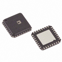
ADN8830ACPZ-REEL Analog Devices Inc, ADN8830ACPZ-REEL Datasheet - Page 20

ADN8830ACPZ-REEL
Manufacturer Part Number
ADN8830ACPZ-REEL
Description
IC THERMO COOLER CNTRLR 32-LFCSP
Manufacturer
Analog Devices Inc
Datasheet
1.ADN8830ACPZ-REEL7.pdf
(24 pages)
Specifications of ADN8830ACPZ-REEL
Applications
Thermoelectric Cooler
Current - Supply
8mA
Voltage - Supply
3.3 V ~ 5 V
Operating Temperature
-40°C ~ 85°C
Mounting Type
Surface Mount
Package / Case
32-LFCSP
Lead Free Status / RoHS Status
Lead free / RoHS Compliant
Other names
ADN8830ACPZ-REELTR
ADN8830
If the voltage at V
VLIM pin will be set to 1.5 V, effectively setting the maximum
voltage across the outputs to 0 V. The voltage divider for V
calculated from Equation 43.
Design Example 5
A maximum output current limit needs to be set at 1.5 A for a
TEC with a maximum voltage rating of 2.5 V. The ADN8830 is
powered from 5 V. The TEC resistance is estimated at 1.67
efficiency at 85%. Using Equation 43, the voltage drop across
R
voltage V
as shown in Figure 21. To set the output voltage limit to 2.5 V,
the voltage at VLIMIT should be set to 0.875 V according to
Equation 17.
The C1 capacitor is added to smooth the voltage transitions at
VLIM. Once an overcurrent condition is detected, the output
voltage will turn down to 0 V within 30 ms.
For a more exact measurement of the output current, place a
sense resistor in series with the output load, as shown in Figure 23.
The AD626 instrumentation amplifier is set for a gain of 100
with a reference voltage of 2.47 V from VREF. The output of
the AD626 is equal to 100 R
which is set up as a window comparator. With V
VLO but less than VHI, VLIM will be pulled down to the volt-
age at VLIMIT. Should V
VLIM will be pulled to 1.5 V as in Figure 21. The trip points
should be set according to
S
will be 8.8 mV when 1.5 A is delivered to the TEC. The trip
VHI
VLO VREF
X
is set to 4.991 V with R3 = 178
VREF
SY
–
drops below V
82.5
100
100
RTD
1k
R3
X
R I
R I
fall outside the voltage window,
S LIMIT
82.5
Figure 22. Using an RTD for Temperature Feedback to the ADN8830
S LIMIT
S
1k
R3
R3
I
L
X
4.99k
and is fed to the AD8602,
, Q1 is turned off and the
–
I
I
OUTB
OUTA
+IN
+IN
RGA
RGB
–IN
OA
IA
IA
and R4 = 100 k
SENSE
GND
X
greater than
INST
AMP
5V
AGND
X
(44)
and
NOTE: ADDITIONAL PINS OMITTED FOR CLARITY
is
–20–
OUT
The upper and lower trip point voltages can be set independently,
allowing different maximum output current limits depending on
the direction of the current. The resistor divider for VHI and
VLO is tapped to VREF to maintain window accuracy with any
changes in VREF. Using the values from Figure 23 with a 5 V
supply, the output current will not exceed 1.5 A in either direction.
Adding the current sensing resistor will slightly reduce efficiency.
The power dissipated by this resistor is D ITEC2
TEC is heating, or (1–D) ITEC2
Include this when calculating efficiency as described in the
Calculating Power Dissipation and Efficiency section.
TEC
TO
1k
IA
Figure 23. High Accuracy Output Current Limit
10m
R
–IN
S
I
L
OA
8
5.11k
TO
OUT B
VREF
AD626
TO
AVDD
ADT70
V
V
1nF
HI
LO
200k
300k
300k
200k
OUT
V
OA
X
AVDD
TO THERM_IN
= 1V @ 25 C
25mV/ C
R
S
AD8602
if the TEC is cooling.
AVDD
FDG6303N
EQUIVA-
3.48k
Q1,Q2
LENT
(0V TO 1.5V)
R1
OR
VLIMIT
R
AVDD
S
REV. C
if the
R2
1.47k
TO
VLIM


