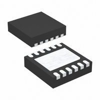
LTC2930HDD#PBF Linear Technology, LTC2930HDD#PBF Datasheet - Page 3

LTC2930HDD#PBF
Manufacturer Part Number
LTC2930HDD#PBF
Description
IC 6 POWER SUPPLY MONITOR 12DFN
Manufacturer
Linear Technology
Datasheet
1.LTC2930HDDPBF.pdf
(12 pages)
Specifications of LTC2930HDD#PBF
Applications
Six Power Supply Monitor
Voltage - Supply
1 V ~ 7 V
Operating Temperature
-40°C ~ 125°C
Mounting Type
Surface Mount
Package / Case
12-DFN
Lead Free Status / RoHS Status
Lead free / RoHS Compliant
Current - Supply
-
Voltage - Input
-
Available stocks
Company
Part Number
Manufacturer
Quantity
Price
ELECTRICAL CHARACTERISTICS
SYMBOL
I
I
I
I
I
I
I
t
t
V
V
V
V
t
t
I
TIMING DIAGRAM
temperature range, otherwise specifi cations are at T
Note 1: Stresses beyond those listed under Absolute Maximum Ratings
may cause permanent damage to the device. Exposure to any Absolute
Maximum Rating condition for extended periods may affect device reliability
and lifetime.
Note 2: All currents into pins are positive, all voltages are referenced to GND
unless otherwise noted.
Note 3: The greater of V1, V2 is the internal supply voltage (V
V1
V2
V3
V4
V5
CRT(UP)
CRT(DN)
RST
UV
MRW
MRD
MR
OL
OH
IL
IH
, I
V6
PARAMETER
V1 Input Current
V2 Input Current
V3 Input Current
V4 Input Current
V5, V6 Input Current
CRT Pull-Up Current
CRT Pull-Down Current
Reset Timeout Period
V
Voltage Output Low RST
Voltage Output High RST (Note 5)
MR Input Threshold Low
MR Input Threshold High
MR Input Pulse Width
Manual Reset Propagation Delay
MR Pull-Up Current
RST
n
MR
V
Undervoltage Detect to RST
n
V
RT
t
UV
A
CC
= 25°C. V
t
).
RST
CONDITIONS
V1 = 5V, I
V2 = 3.3V
V3 = 2.5V
V3 = 0.55V (ADJ Mode)
V4 = 1.8V
V4 = 0.55V (ADJ Mode)
V4 = –0.02V (–ADJ Mode)
V5, V6 = 0.55V
V
V
C
V
than 1%
I
I
I
V
V
V
V
V
SINK
SINK
SOURCE
CRT
CRT
RT
n
CC
CC
CC
CC
MR
V
Less Than Reset Threshold by More
The
= 1500pF
= 3.3V to 5.5V
= 3.3V to 5.5V
= 3.3V
= 3.3V, V
n
= 1V
= GND
= 1.3V
= 3mA, V
= 100μA, V
Monitor Timing
= –1μA
●
CC
VREF
denotes the specifi cations which apply over the full operating
= 5V, unless otherwise specifi ed. (Note 3)
MR
= 12μA (Note 4)
CC
Note 4: Under static no-fault conditions, V1 will necessarily supply quiescent
current. If at any time V2 is larger than V1, V2 must be capable of supplying
the quiescent current, programming (transient) current and reference load
current.
Note 5: The output pin RST has a diode protected internal pull-up to V2 of
typically 6μA. However, an external pull-up resistor may be used when faster
rise times are required or for V
CC
Falling
= 3V
= 1V
t
MRW
t
MRD
●
●
●
●
●
●
●
●
●
●
●
●
●
●
●
●
●
●
●
OH
t
RST
voltages greater than V2.
V2-1
MIN
–1.4
150
1.6
10
–4
2
2930 TD
0.52
0.34
0.15
0.05
TYP
150
–10
0.8
0.1
52
–2
20
3
LTC2930
MAX
–2.6
±15
±15
±15
±15
–16
1.2
0.8
0.4
0.3
0.4
75
30
2
4
1
UNITS
2930fa
3
ms
μA
μA
μA
nA
μA
nA
nA
nA
μA
μA
μA
μs
ns
μs
V
V
V
V
V


