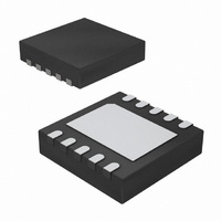
IR3720MTRPBF International Rectifier, IR3720MTRPBF Datasheet - Page 6

IR3720MTRPBF
Manufacturer Part Number
IR3720MTRPBF
Description
IC POWER SUPPLY MONITOR 10-DFN
Manufacturer
International Rectifier
Series
TruePower™r
Datasheet
1.IR3720MTRPBF.pdf
(20 pages)
Specifications of IR3720MTRPBF
Package / Case
10-DFN
Mounting Type
Surface Mount
Current - Supply
480µA
Voltage - Supply
3.135 V ~ 3.465 V
Operating Temperature
0°C ~ 125°C
Applications
Power Supply Monitor
Voltage - Input
-
Input Voltage
3.3V
No. Of Outputs
1
Supply Voltage Range
3.135V To 3.465V
No. Of Pins
10
Operating Temperature Range
0°C To +125°C
Filter Terminals
SMD
Input Voltage Primary Max
3.3V
Rohs Compliant
Yes
Frequency
400kHz
Package
10 Lead 3x3 DFN
Vk Range
0.5V - 1.8V
Bias Supply Voltage
+3.3V +/-5%
Junction Temperature
0oC to 125oC
Pbf
Yes
Lead Free Status / RoHS Status
Lead free / RoHS Compliant
Voltage - Input
-
Lead Free Status / Rohs Status
Lead free / RoHS Compliant
Available stocks
Company
Part Number
Manufacturer
Quantity
Price
Company:
Part Number:
IR3720MTRPBF
Manufacturer:
WIMA
Quantity:
1 200
IC PIN FUNCTIONS
VDD PIN
This pin provides operational bias current to circuits
internal to the IR3720. Bypass it with a high quality
ceramic capacitor to the GND pin.
GND PIN
This pin returns operational bias current to its source.
It is also the reference to which the voltage VO is
measured, and it sinks the reference current
established by the external resistor R
VO PIN
Connect this pin to the location in the circuit where
voltage for the power calculation is desired to be
monitored. Since it also measures DCR voltage drop
it is critical that it be Kelvin connected to the buck
inductor output. Power accuracy may be degraded if
the voltage at this pin is below VO
VCS PIN
The average current into this pin is used to calculate
power. A switched current source internal to the
IR3720 will maintain the average voltage of this pin
equal to the voltage of the VO pin.
VREF FUNCTION
A voltage reference internal to the IR3720 drives the
V
to set the amplitude of the current monitor switched
current source I
GND through a precision resistor network R
network may include provision for canceling the
positive temperature coefficient of the buck inductor’s
DC resistance (DCR).
ALERT# FUNCTION
The ALERT# pin is a multi-use pin. During normal
use it can be configured via the I
ALERT# pin that will be driven logic low when new
data is available in the output register. After the
output register has been read via the I
will be released to its high resistance state. This pin
can also be programmed to pull low when the output
exceeds the programmable level.
Page 6 of 20
REF
pin while the pin current is monitored and used
REF
. This pin should be connected to
2
C as an open drain
min
.
T
2
.
C the ALERT#
www.irf.com
T
. This
ADDR PIN
The ADDR pin is an input that establishes the I
address. Valid addresses are selected by grounding,
floating, or wiring to VDD the ADDR pin. Table 1,
“User Selectable Addresses”, provides a mapping of
possible selections.
Table 1 User selectable addresses
ADDR pin configuration
Low
Open
High
EXTCLK
This pin is a Schmitt trigger input for an optional
externally provided square wave clock. The duty ratio
of this externally provided clock, if used, shall be
between 40% and 60%. If no external clock is used,
connect this pin to GND and the internal clock will be
used.
SCL
SCL is the I
with a rate as low as 10 kHz. It will continue to
function as the rate is increased to 400 kHz. This
device is considered a slave, and therefore uses the
SCL as an input only.
SDA
SDA is monitored as data input during master to
slave transactions, and is driven as data output
during slave to master transactions as indicated in
the Packet Protocol section to follow.
2
C clock and is capable of functioning
I
b’1110 000
b’1110 010
b’1110 110
2
C Address
DATA SHEET
IR3720
09/09/08
2
C


