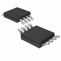
LTC1966CMS8 Linear Technology, LTC1966CMS8 Datasheet - Page 24

LTC1966CMS8
Manufacturer Part Number
LTC1966CMS8
Description
IC PREC RMS/DC CONV MCRPWR 8MSOP
Manufacturer
Linear Technology
Datasheet
1.LTC1966CMS8.pdf
(32 pages)
Specifications of LTC1966CMS8
Current - Supply
155µA
Voltage - Supply
2.7 V ~ 5.5 V
Mounting Type
Surface Mount
Package / Case
8-MSOP, Micro8™, 8-uMAX, 8-uSOP,
Lead Free Status / RoHS Status
Contains lead / RoHS non-compliant
Available stocks
Company
Part Number
Manufacturer
Quantity
Price
Part Number:
LTC1966CMS8
Manufacturer:
LINEAR/凌特
Quantity:
20 000
Company:
Part Number:
LTC1966CMS8#PBF/H/MP
Manufacturer:
LT
Quantity:
2 335
APPLICATIO S I FOR ATIO
LTC1966
small, 2.5pF • 100k = 250ns, and during the 2.5 s period
devoted to sampling, ten time constants elapse. This
allows each sample to settle to within 46ppm and it is these
samples that are used to compute the RMS value.
This is a much higher accuracy than the LTC1966 conver-
sion limits, and far better than the accuracy computed via
the simplistic resistive divider model:
This resistive divider calculation does give the correct
model of what voltage is seen at the input terminals by a
parallel load averaged over a several clock cycles, which is
what a large shunt capacitor will do—average the current
spikes over several clock cycles.
When high source impedances are used, care must be taken
to minimize shunt capacitance at the LTC1966 input so as
not to increase the settling time. Shunt capacitance of just
2.5pF will double the input settling time constant and the
error in the above example grows from 46ppm to 0.67%
(6700ppm). A 13pF scope probe will increase the error to
almost 20%. As a consequence, it is important to not try
to filter the input with large input capacitances unless driven
by a low impedance. Keep time constant << 2.5 s.
When the LTC1966 is driven by op amp outputs, whose
low DC impedance can be compromised by sharp capaci-
tive load switching, a small series resistor may be added.
A 10k resistor will easily settle with the 2.5pF input
sampling capacitor to within 1ppm.
These are important points to consider both during design
and debug. During lab debug, and even production testing,
a high value series resistor to any test point is advisable.
24
V
IN
V
V
V
SOURCE
SOURCE
SOURCE
U
8
– . %
R
M
IN
1 25
8
U
R
R
M
IN
SOURCE
100
k
W
U
Output Impedance
The LTC1966 output impedance during operation is simi-
larly due to a switched capacitor action. In this case, 59pF
of on-chip capacitance operating at 100kHz translates into
170k . The closed-loop RMS-to-DC calculation cuts that
in half to the nominal 85k specified.
In order to create a DC result, a large averaging capacitor
is required. Capacitive loading and time constants are not
an issue on the output.
However, resistive loading is an issue and the 10M
impedance of a DMM or 10 scope probe will drag the
output down by –0.85% typ.
During shutdown, the switching action is halted and a
fixed 30k resistor shunts V
discharged.
Interfacing with an ADC
The LTC1966 output impedance and the RMS averaging
ripple need to be considered when using an analog-to-
digital converter (ADC) to digitize the LTC1966 RMS
result.
The simplest configuration is to connect the LTC1966
directly to the input of a type 7106/7136 ADC as shown in
Figure 22a. These devices are designed specifically for
DVM/DPM use and include display drivers for a 3 1/2 digit
LCD segmented display. Using a dual-slope conversion,
the input is sampled over a long integration window, which
results in rejection of line frequency ripple when integra-
tion time is an integer number of line cycles. Finally, these
parts have an input impedance in the G
specified input leakage of 10pA to 20pA. Such a leakage,
combined with the LTC1966 output impedance, results in
just 1 V to 2 V of additional output offset voltage.
Another type of ADC that has inherent rejection of RMS
averaging ripple is an oversampling
LTC2420. Its input impedance is 6.5M , but only when it
is sampling. Since this occurs only half the time at most,
if it directly loads the LTC1966, a gain error of – 0.54% to
– 0.73% results. In fact, the LTC2420 DC input current is
not zero at 0V, but rather at one half its reference, so both
OUT
to OUT RTN so that C
ADC such as the
range, with
sn1966 1966fas
AVE
is


