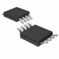
LTC1966CMS8 Linear Technology, LTC1966CMS8 Datasheet - Page 4

LTC1966CMS8
Manufacturer Part Number
LTC1966CMS8
Description
IC PREC RMS/DC CONV MCRPWR 8MSOP
Manufacturer
Linear Technology
Datasheet
1.LTC1966CMS8.pdf
(32 pages)
Specifications of LTC1966CMS8
Current - Supply
155µA
Voltage - Supply
2.7 V ~ 5.5 V
Mounting Type
Surface Mount
Package / Case
8-MSOP, Micro8™, 8-uMAX, 8-uSOP,
Lead Free Status / RoHS Status
Contains lead / RoHS non-compliant
Available stocks
Company
Part Number
Manufacturer
Quantity
Price
Part Number:
LTC1966CMS8
Manufacturer:
LINEAR/凌特
Quantity:
20 000
Company:
Part Number:
LTC1966CMS8#PBF/H/MP
Manufacturer:
LT
Quantity:
2 335
ELECTRICAL CHARACTERISTICS
LTC1966
Note 11: High speed automatic testing cannot be performed with 60Hz
inputs. The LTC1966 is 100% tested with DC stimulus. Correlation tests
have shown that the performance limits above can be guaranteed with the
additional testing being performed to verify proper operation of all internal
circuitry.
Note 12: The LTC1966 is a switched capacitor device and the input/output
impedance is an average impedance over many clock cycles. The input
impedance will not necessarily lead to an attenuation of the input signal
measured. Refer to the Applications Information section titled “Input
Impedance” for more information.
Note 13: The common mode rejection ratios of the LTC1966 are measured
with DC inputs from 50mV to 350mV. The input CMRR is defined as the
change in V
input levels of V
output CMRR is defined as the change in V
V
TYPICAL PERFOR A CE CHARACTERISTICS
4
SS
and OUT RTN = V
IOS
measured between input levels of V
DD
– 350mV to V
–0.1
–0.2
–0.3
–0.4
–0.5
–0.1
–0.2
–0.3
–0.4
–0.5
0.5
0.4
0.3
0.2
0.1
0.5
0.4
0.3
0.2
0.1
DD
0
0
0
0
Gain and Offset
vs Output Common Mode
Gain and Offset
vs Input Common Mode
– 350mV divided by V
V
V
V
V
DD
SS
DD
SS
0.5
0.5
= GND
= GND
= 5V
= 5V
1.0
1.0
OUTPUT COMMON MODE (V)
DD
INPUT COMMON MODE (V)
1.5
1.5
divided by V
W
V
IOS
2.0 2.5
2.0 2.5
GAIN ERROR
OOS
U
GAIN ERROR
V
OOS
DD
3.0 3.5 4.0
3.0 3.5 4.0
measured with OUT RTN =
DD
V
– V
V
SS
OOS
IOS
– V
SS
to V
SS
– 350mV.
SS
– 350mV. The
4.5
1966 G02
4.5
1966 G05
+ 350mV and
5.0
5.0
0.5
0.4
0.3
0.2
0.1
0
–0.1
–0.2
–0.3
–0.4
–0.5
0.5
0.4
0.3
0.2
0.1
0
–0.1
–0.2
–0.3
–0.4
–0.5
Note 14: The LTC1966 input and output voltage swings are limited by
internal clipping. However, its
momentary internal clipping. The input clipping is tested with a crest
factor of 2, while the output clipping is tested with a DC input.
Note 15: The LTC1966 exploits oversampling and noise shaping to reduce
the quantization noise of internal 1-bit analog-to-digital conversions. At
higher input frequencies, increasingly large portions of this noise are
aliased down to DC. Because the noise is shifted in frequency, it becomes
a low frequency rumble and is only filtered at the expense of increasingly
long settling times. The LTC1966 is inherently wideband, but the output
accuracy is degraded by this aliased noise. These specifications apply with
C
Note 16: The LTC1966 can operate down to 2.7V single supply but cannot
operate at 2.7V. This additional constraint on V
mathematically as – 3 • (V
AVE
–0.1
–0.2
–0.3
–0.4
–0.5
–0.1
–0.2
–0.3
–0.4
–0.5
= 10 F and constitute a 3-sigma variation of the output rumble.
0.5
0.4
0.3
0.2
0.1
0.5
0.4
0.3
0.2
0.1
0
0
–5
–5
Gain and Offset
vs Input Common Mode
Gain and Offset
vs Output Common Mode
V
V
V
V
GAIN ERROR
DD
SS
DD
SS
–4
–4
= –5V
= 5V
= –5V
= 5V
V
V
GAIN ERROR
OOS
IOS
–3
–3
OUTPUT COMMON MODE (V)
INPUT COMMON MODE (V)
–2
–2
–1
–1
DD
V
IOS
0
0
– 2.7V) V
1
1
topology is relatively tolerant of
2
2
3
SS
3
1966 G03
V
1966 G06
4
OOS
4
Ground.
5
5
SS
0.5
0.4
0.3
0.2
0.1
0
–0.1
–0.2
–0.3
–0.4
–0.5
0.5
0.4
0.3
0.2
0.1
0
–0.1
–0.2
–0.3
–0.4
–0.5
can be expressed
sn1966 1966fas


