AD595CQ Analog Devices Inc, AD595CQ Datasheet - Page 7
AD595CQ
Manufacturer Part Number
AD595CQ
Description
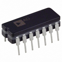
IC THERMOCOUPLE A W/COMP 14CDIP
Manufacturer
Analog Devices Inc
Type
Low Powerr
Specifications of AD595CQ
Rohs Status
RoHS non-compliant
Function
Thermocouple Amplifier
Topology
Ice Point Compensation, Overload Detection
Sensor Type
External
Output Type
Voltage
Output Alarm
Yes
Output Fan
No
Voltage - Supply
5 V ~ ±15 V
Operating Temperature
-55°C ~ 125°C
Mounting Type
Through Hole
Package / Case
14-CDIP (0.300", 7.62mm)
Ic Output Type
Voltage
Sensing Accuracy Range
± 1°C
Supply Current
160µA
Supply Voltage Range
5V To 30V
Sensor Case Style
DIP
No. Of Pins
14
Termination Type
DIP
Amplifier Type
Instrumentation
Bandwidth
15 kHz
Converter Type
Monolithic theremocouple amplifier
Current, Input Bias
0.1 μA
Current, Output
±5 mA
Current, Quiescent Supply
160 uA (Typ.) @ 25 °C
Current, Supply
160 μA
Package Type
CDIP-14
Temperature, Operating, Maximum
125 °C
Temperature, Operating, Minimum
-55 °C
Temperature, Operating, Range
-55 to +125 °C
Voltage, Supply
+5 to ±15 V
Low Impedance Voltage Output
10 mV⁄°C
Wide Power Supply Range
+ 5 V to 615 V
Low Power
1 mW typical
Filter Terminals
DIP
Rohs Compliant
No
Accuracy
± 1
Accuracy %
1%
Sensing Temperature
-
Lead Free Status / RoHS Status
Contains lead / RoHS non-compliant
Available stocks
Company
Part Number
Manufacturer
Quantity
Price

Part Number:
AD595CQ
Manufacturer:
ADI/亚德诺
Quantity:
20 000
Company:
Part Number:
AD595CQZ
Manufacturer:
AMI
Quantity:
6 242


ALARM CIRCUIT
In all applications of the AD594/AD595 the –ALM connection,
Pin 13, should be constrained so that it is not more positive
than (V+) – 4 V. This can be most easily achieved by connect-
ing Pin 13 to either common at Pin 4 or V– at Pin 7. For most
applications that use the alarm signal, Pin 13 will be grounded
and the signal will be taken from +ALM on Pin 12. A typical
application is shown in Figure 10.
In this configuration the alarm transistor will be off in normal
operation and the 20 k pull up will cause the +ALM output on
Pin 12 to go high. If one or both of the thermocouple leads are
interrupted, the +ALM pin will be driven low. As shown in Fig-
ure 10 this signal is compatible with the input of a TTL gate
which can be used as a buffer and/or inverter.
Since the alarm is a high level output it may be used to directly
drive an LED or other indicator as shown in Figure 11.
A 270
but may be omitted since the alarm output transistor is current
limited at about 20 mA. The transistor, however, will operate in
a high dissipation mode and the temperature of the circuit will
rise well above ambient. Note that the cold junction compensa-
tion will be affected whenever the alarm circuit is activated. The
time required for the chip to return to ambient temperature will
depend on the power dissipation of the alarm circuit, the nature
of the thermal path to the environment and the alarm duration.
REV. C
Figure 10. Using the Alarm to Drive a TTL Gate
(“Grounded’’ Emitter Configuration)
CONSTANTAN
(ALUMEL)
IRON
(CHROMEL)
CONSTANTAN
(ALUMEL)
series resistor will limit current in the LED to 10 mA,
IRON
(CHROMEL)
Figure 11. Alarm Directly Drives LED
14
1
AD594/
AD595
14
1
G
AD594/
AD595
20k
13
2
G
COMMON
LED
270
13
2
12
3
12
3
OVERLOAD
DETECT
G
V+
11
4
OVERLOAD
DETECT
ALARM OUT
G
11
4
+A
10
5
+A
+TC
10
5
+TC
6
9
COMP.
POINT
ICE
9
6
POINT
COMP.
ICE
8
7
–TC
8
7
10mV/ C
–TC
ALARM
TTL GATE
10mV/ C
GND
+5V
–7–
The alarm can be used with both single and dual supplies. It
can be operated above or below ground. The collector and emit-
ter of the output transistor can be used in any normal switch
configuration. As an example a negative referenced load can be
driven from –ALM as shown in Figure 12.
The collector (+ALM) should not be allowed to become more
positive than (V–) +36 V, however, it may be permitted to be
more positive than V+. The emitter voltage (–ALM) should be
constrained so that it does not become more positive than 4
volts below the V+ applied to the circuit.
Additionally, the AD594/AD595 can be configured to produce
an extreme upscale or downscale output in applications where
an extra signal line for an alarm is inappropriate. By tying either
of the thermocouple inputs to common most runaway control
conditions can be automatically avoided. A +IN to common
connection creates a downscale output if the thermocouple opens,
while connecting –IN to common provides an upscale output.
CELSIUS THERMOMETER
The AD594/AD595 may be configured as a stand-alone Celsius
thermometer as shown in Figure 13.
Simply omit the thermocouple and connect the inputs (Pins 1
and 14) to common. The output now will reflect the compensa-
tion voltage and hence will indicate the AD594/AD595
temperature with a scale factor of 10 mV/ C. In this three termi-
nal, voltage output, temperature sensing mode, the AD594/
AD595 will operate over the full military –55 C to +125 C tem-
perature range.
ALARM
RELAY
Figure 13. AD594/AD595 as a Stand-Alone Celsius
Thermometer
Figure 12. –ALM Driving A Negative Referenced Load
CONSTANTAN
(ALUMEL)
IRON
(CHROMEL)
14
1
AD594/
AD595
G
13
2
12
3
OVERLOAD
DETECT
14
G
1
11
4
AD594/
AD595
G
+A
13
2
10
5
+TC
12
3
9
6
COMP.
POINT
ICE
OVERLOAD
DETECT
AD594/AD595
G
11
4
8
7
–TC
+A
10
5
+TC
OUTPUT
10mV/ C
9
6
COMP.
POINT
+5V TO +15V
0 TO –15V
GND
ICE
7
8
–TC
10mV/ C
–12V
GND
+10V
Related parts for AD595CQ
Image
Part Number
Description
Manufacturer
Datasheet
Request
R

Part Number:
Description:
±1.7g Dual-Axis IMEMS Accelerometer Evaluation Board
Manufacturer:
Analog Devices Inc
Datasheet:

Part Number:
Description:
Inertial Sensor Evaluation System
Manufacturer:
Analog Devices Inc
Datasheet:
Part Number:
Description:
Manufacturer:
Analog Devices Inc
Datasheet:
Part Number:
Description:
Manufacturer:
Analog Devices Inc
Datasheet:
Part Number:
Description:
Manufacturer:
Analog Devices Inc
Datasheet:
Part Number:
Description:
Manufacturer:
Analog Devices Inc
Datasheet:
Part Number:
Description:
Manufacturer:
Analog Devices Inc
Datasheet:
Part Number:
Description:
Manufacturer:
Analog Devices Inc
Datasheet:
Part Number:
Description:
Manufacturer:
Analog Devices Inc
Datasheet:
Part Number:
Description:
Manufacturer:
Analog Devices Inc
Datasheet:
Part Number:
Description:
Manufacturer:
Analog Devices Inc
Datasheet:
Part Number:
Description:
Manufacturer:
Analog Devices Inc
Datasheet:
Part Number:
Description:
Manufacturer:
Analog Devices Inc
Datasheet: