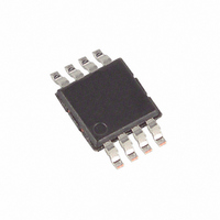
DS1825U+ Maxim Integrated Products, DS1825U+ Datasheet

DS1825U+
Specifications of DS1825U+
Related parts for DS1825U+
DS1825U+ Summary of contents
Page 1
... ORDERING INFORMATION ORDERING NUMBER DS1825U 1825 DS1825U/T&R 1825 DS1825U+ 1825 (See Note 1) DS1825U+T&R 1825 (See Note 1) Note 1: Additionally, a "+" symbol will be marked on the package. Programmable Resolution 1-Wire Digital Thermometer With 4-Bit ID PIN ASSIGNMENT PIN DESCRIPTION GND DQ N.C. ...
Page 2
DESCRIPTION (cont.) Each DS1825 has a unique 64-bit serial code, which allows multiple DS1825s to function on the same 1-Wire bus; thus simple to use one microprocessor to control many DS1825s distributed over a large area. In addition, ...
Page 3
AC ELECTRICAL CHARACTERISTICS: NV MEMORY PARAMETER NV Write Cycle Time EEPROM Writes EEPROM Data Retention AC ELECTRICAL CHARACTERISTICS PARAMETER Temperature Conversion Time Time to Strong Pullup On Time Slot Recovery Time Write 0 Low Time Write 1 Low Time Read ...
Page 4
OVERVIEW Figure 1 shows a block diagram of the DS1825, and pin descriptions are given in Table 1. The 64-bit ROM stores the device’s unique serial code. The scratchpad memory contains the 2-byte temperature register that stores the digital output ...
Page 5
OPERATION¾MEASURING TEMPERATURE The core functionality of the DS1825 is its direct-to-digital temperature sensor. The resolution of the temperature sensor is user-configurable to 9, 10, 11 bits, corresponding to increments of 0.5°C, 0.25°C, 0.125°C, and 0.0625°C, respectively. The default ...
Page 6
Figure 3. T AND T REGISTER FORMAT H L bit 7 bit Only bits 11 through 4 of the temperature register are used in the T registers. If the measured temperature is lower than or equal ...
Page 7
Figure 4. SUPPLYING THE PARASITE-POWERED DS1825 DURING TEMPERATURE CONVERSIONS Micro- processor Figure 5. POWERING THE DS1825 WITH AN EXTERNAL SUPPLY Micro- processor 64-BIT LASERED ROM CODE Each DS1825 contains a unique 64-bit code (see Figure 6) stored in ROM. The ...
Page 8
Byte 8 of the scratchpad is read-only and contains the cyclic redundancy check (CRC) code for bytes 0 through 7 of the scratchpad. The DS1825 generates this CRC using the method described in the CRC GENERATION section. Data is written ...
Page 9
Table 4. THERMOMETER RESOLUTION CONFIGURATION CRC GENERATION CRC bytes are provided as part of the DS1825’s 64-bit ROM code and in the 9 The ROM code CRC is calculated from the first 56 bits of ...
Page 10
HARDWARE CONFIGURATION The 1-Wire bus has by definition only a single data line. Each device (master or slave) interfaces to the data line through an open-drain or 3-state port. This allows each device to “release” the data line when the ...
Page 11
SEARCH ROM [F0h] When a system is initially powered up, the master must identify the ROM codes of all slave devices on the bus, which allows the master to determine the number of slaves and their device types. The master ...
Page 12
READ SCRATCHPAD [BEh] This command allows the master to read the contents of the scratchpad. The data transfer starts with the least significant bit of byte 0 and continues through the scratchpad until the 9 may issue a reset to ...
Page 13
Figure 11. ROM COMMANDS FLOW CHART Initialization Sequence 33h N READ ROM COMMAND Y DS1825 T X FAMILY CODE 1 BYTE DS1825 T X SERIAL NUMBER 6 BYTES DS1825 T X CRC BYTE MASTER T X RESET PULSE DS1825 T ...
Page 14
Figure 12. DS1825 FUNCTION COMMANDS FLOW CHART 44h MASTER T CONVERT X FUNCTION TEMPERATURE COMMAND ? Y N PARASITE POWER ? DS1825 BEGINS CONVERSION DEVICE N CONVERTING TEMPERATURE ? Y MASTER MASTER R “0s” R “1s” B4h N ...
Page 15
SUGGESTED PROCEDURE FOR BUILDING CROSS-REFERENCE TABLE This procedure uses the Search ROM command to find all DS1825s on the one-wire bus (16 maximum) and then reads each configuration register to match the ROMIDs to the hard-wired addresses. Figure 13 Increment ...
Page 16
SIGNALING The DS1825 uses a strict 1-Wire communication protocol to insure data integrity. Several signal types are defined by this protocol: reset pulse, presence pulse, write 0, write 1, read 0, and read 1. All of these signals, with ...
Page 17
Figure 15. READ/WRITE TIME SLOT TIMING DIAGRAM START OF SLOT MASTER WRITE “0” SLOT 60 ms < 1-WIRE BUS GND 15 ms MASTER READ “0” SLOT V PU 1-WIRE BUS GND > LINE ...
Page 18
Figure 16. DETAILED MASTER READ 1 TIMING V PU 1-WIRE BUS GND T INT Figure 17. RECOMMENDED MASTER READ 1 TIMING V PU 1-WIRE BUS GND INT RC small small DS1825 OPERATION EXAMPLE In this example ...
Page 19
Figure 18. TYPICAL PERFORMANCE CURVE -1 Figure 19. TIMING DIAGRAMS 1 +3σ 0 -3σ - Temperature, Degrees Centigrade ...
Page 20
Figure 20. ADDRESS PROGRAMMING DIAGRAM, V 1-Wire Bus Note: AD0-AD3 cannot float, each pin must be tied to either V Location 0 DQ AD0 AD1 VDD VDD AD2 GND AD3 VDD Location 1 DQ AD0 AD1 VDD AD2 GND AD3 ...
Page 21
Figure 21. ADDRESS PROGRAMMING DIAGRAM, PARASITE POWERED 1-Wire Bus Note: AD0-AD3 cannot float, each pin must be tied to either V Location 0 DQ AD0 ADO = GND AD1 AD1 = GND VDD AD2 AD2 = GND GND AD3 AD3 ...


