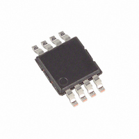
DS1825U+ Maxim Integrated Products, DS1825U+ Datasheet - Page 7

DS1825U+
Manufacturer Part Number
DS1825U+
Description
IC THERMOMETER DIGITAL 8-USOP
Manufacturer
Maxim Integrated Products
Datasheet
1.DS1825U.pdf
(21 pages)
Specifications of DS1825U+
Function
Thermometer, Thermostat
Topology
Register Bank, Scratchpad
Sensor Type
Internal
Sensing Temperature
-55°C ~ 125°C
Output Type
Digital
Output Alarm
Yes
Output Fan
No
Voltage - Supply
3 V ~ 3.7 V
Operating Temperature
-55°C ~ 125°C
Mounting Type
Surface Mount
Package / Case
8-MSOP, Micro8™, 8-uMAX, 8-uSOP,
Temperature Threshold
Programmable
Full Temp Accuracy
+/- 0.5 C
Digital Output - Bus Interface
1-Wire
Digital Output - Number Of Bits
9 bit to 12 bit
Supply Voltage (max)
3.7 V
Supply Voltage (min)
3 V
Maximum Operating Temperature
+ 125 C
Minimum Operating Temperature
- 55 C
Supply Current
1.5 mA
Ic Output Type
Digital
Sensing Accuracy Range
± 0.5°C
Supply Voltage Range
3V To 3.7V
Resolution (bits)
12bit
Sensor Case Style
µSOP
No. Of Pins
8
Accuracy %
0.5°C
Rohs Compliant
Yes
Lead Free Status / RoHS Status
Lead free / RoHS Compliant
Figure 4. SUPPLYING THE PARASITE-POWERED DS1825 DURING
TEMPERATURE CONVERSIONS
Figure 5. POWERING THE DS1825 WITH AN EXTERNAL SUPPLY
64-BIT LASERED ROM CODE
Each DS1825 contains a unique 64-bit code (see Figure 6) stored in ROM. The least significant 8 bits of the ROM
code contain the DS1825’s 1-Wire family code: 3Bh. The next 48 bits contain a unique serial number. The most
significant 8 bits contain a cyclic redundancy check (CRC) byte that is calculated from the first 56 bits of the ROM
code. A detailed explanation of the CRC bits is provided in the CRC GENERATION section. The 64-bit ROM code
and associated ROM function control logic allow the DS1825 to operate as a 1-Wire device using the protocol
detailed in the 1-Wire BUS SYSTEM section of this data sheet.
Figure 6. 64-BIT LASERED ROM CODE
MEMORY
The DS1825’s memory is organized as shown in Figure 7. The memory consists of an SRAM scratchpad with NV
EEPROM storage for the high and low alarm trigger registers (T
DS1825 alarm function is not used, the T
commands are described in detail in the DS1825 FUNCTION COMMANDS section.
Byte 0 and byte 1 of the scratchpad contain the LSB and the MSB of the temperature register, respectively. These
bytes are read-only. Bytes 2 and 3 provide access to T
data, which is explained in detail in the CONFIGURATION REGISTER section of this data sheet. Bytes 5, 6, and 7
are reserved for internal use by the device and cannot be overwritten.
MSB
8-BIT CRC
processor
Micro-
processor
Micro-
LSB
V
PU
V
MSB
PU
4.7K
4.7K
H
48-BIT SERIAL NUMBER
and T
1-Wire Bus
L
registers can serve as general-purpose memory. All memory
7 of 21
H
and T
V
PU
1-Wire Bus
L
GND
H
registers. Byte 4 contains the configuration register
and T
DS1825
DQ
L
LSB
) and configuration register. Note that if the
V
GND
DD
DS1825
MSB
DQ
V
8-BIT FAMILY CODE (3Bh)
DD
V
(External Supply)
DD
To Other
1-Wire Devices
To Other
1-Wire Devices
LSB


