AD594ADZ Analog Devices Inc, AD594ADZ Datasheet - Page 2
AD594ADZ
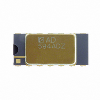
Manufacturer Part Number
AD594ADZ
Description
IC THERMOCOUPLE INSTR AMP 14CDIP
Manufacturer
Analog Devices Inc
Datasheet
1.AD595AQ.pdf
(8 pages)
Specifications of AD594ADZ
Function
Thermocouple Amplifier
Topology
Ice Point Compensation, Overload Detection
Sensor Type
External
Output Type
Voltage
Output Alarm
Yes
Output Fan
No
Voltage - Supply
5 V ~ ±15 V
Operating Temperature
-55°C ~ 125°C
Mounting Type
Through Hole
Package / Case
14-CDIP (0.300", 7.62mm)
Temperature Sensor Function
Temp Sensor
Operating Temperature (max)
125C
Operating Temperature Classification
Military
Operating Supply Voltage (typ)
5V
Operating Supply Voltage (max)
5.5V
No. Of Amplifiers
2
Input Offset Voltage
16µV
Bandwidth
15kHz
Amplifier Output
Single Ended
Supply Voltage Range
5V To ± 15V
Supply Current
160µA
Amplifier Case Style
TO-116
Rohs Compliant
Yes
Lead Free Status / RoHS Status
Lead free / RoHS Compliant
Sensing Temperature
-
Lead Free Status / Rohs Status
Compliant


AD594/AD595–SPECIFICATIONS
Model
ABSOLUTE MAXIMUM RATING
TEMPERATURE MEASUREMENT
AMPLIFIER CHARACTERISTICS
ALARM CHARACTERISTICS
POWER REQUIREMENTS
PACKAGE OPTION
NOTES
1
2
3
4
5
Specifications shown in boldface are tested on all production units at final electrical test. Results from those tests are used to calculate outgoing quality levels. All min and max specifications
are guaranteed, although only those shown in boldface are tested on all production units.
Specifications subject to change without notic
INTERPRETING AD594/AD595 OUTPUT VOLTAGES
To achieve a temperature proportional output of 10 mV/ C and
accurately compensate for the reference junction over the rated
operating range of the circuit, the AD594/AD595 is gain trimmed
to match the transfer characteristic of J and K type thermocouples
at 25 C. For a type J output in this temperature range the TC is
51.70 V/ C, while for a type K it is 40.44 V/ C. The resulting
gain for the AD594 is 193.4 (10 mV/ C divided by 51.7 V/ C)
and for the AD595 is 247.3 (10 mV/ C divided by 40.44 V/ C).
In addition, an absolute accuracy trim induces an input offset to
the output amplifier characteristic of 16 V for the AD594 and
11 V for the AD595. This offset arises because the AD594/
AD595 is trimmed for a 250 mV output while applying a 25 C
thermocouple input.
Because a thermocouple output voltage is nonlinear with respect
to temperature, and the AD594/AD595 linearly amplifies the
Calibrated for minimum error at +25 C using a thermocouple sensitivity of 51.7 V/ C. Since a J type thermocouple deviates from this straight line approximation, the AD594 will normally
Defined as the slope of the line connecting the AD594/AD595 errors measured at 0 C and 50 C ambient temperature.
Pin 8 shorted to Pin 9.
Current Sink Capability in single supply configuration is limited to current drawn to ground through a 50 k resistor at output voltages below 2.5 V.
–V
read 3.1 mV when the measuring junction is at 0 C. The AD595 will similarly read 2.7 mV at 0 C.
+V
Common-Mode Input Voltage
Differential Input Voltage
Alarm Voltages
Operating Temperature Range
Output Short Circuit to Common
(Specified Temperature Range
0 C to +50 C)
Closed Loop Gain
Input Offset Voltage
Input Bias Current
Differential Input Range
Common-Mode Range
Common-Mode Sensitivity – RTO
Power Supply Sensitivity – RTO
Output Voltage Range
Usable Output Current
3 dB Bandwidth
V
Leakage Current
Operating Voltage at – ALM
Short Circuit Current
Specified Performance
Operating
Quiescent Current (No Load)
TO-116 (D-14)
Cerdip (Q-14)
S
CE(SAT)
must not exceed –16.5 V.
S
+ALM
–ALM
Calibration Error at +25 C
Stability vs. Temperature
Gain Error
Nominal Transfer Function
Dual Supply
Single Supply
+V
–V
to –V
S
S
at 2 mA
5
S
3
4
2
1
Min
–V
–V
–V
–V
–55
Indefinite
–10
–V
–V
0
S
S
S
S
S
S
e.
– 0.15
+ 2.5
– 0.15
(Temperature in C)
51.70 V/ C
+V
+V
S
S
AD594AD
AD594AQ
= 5, –V
to –V
AD594A
Typ
193.4
0.1
15
0.3
20
160
100
5
S
S
= 0
30
Max
36
+V
+V
–V
+V
+125
10
+50
–V
10
10
+V
+V
+V
300
3
0.05
1.5
1
S
S
S
S
S
S
S
S
– 4
+ 36
– 2
– 2
– 4
Min
–V
–V
–V
–V
–55
Indefinite
–V
–V
0
(Temperature in C)
51.70 V/ C
S
S
S
S
S
S
– 0.15
– 0.15
+ 2.5
+V
+V
AD594CD
AD594CQ
S
S
= 5, –V
to –V
AD594C
Typ
0.1
15
0.3
20
160
100
5
(@ +25 C and V
unless otherwise noted)
S
–2–
S
= 0
30
compensated signal, the following transfer functions should be
used to determine the actual output voltages:
Table I lists the ideal AD594/AD595 output voltages as a func-
tion of Celsius temperature for type J and K ANSI standard
thermocouples, with the package and reference junction at
25 C. As is normally the case, these outputs are subject to cali-
bration, gain and temperature sensitivity errors. Output values
for intermediate temperatures can be interpolated, or calculated
using the output equations and ANSI thermocouple voltage
tables referred to zero degrees Celsius. Due to a slight variation
in alloy content between ANSI type J and DIN F
Max
36
+V
+V
–V
+V
+125
10
193.4
–V
10
10
+V
–V
+V
300
1
0.025
0.75
1
S
S
AD595 output = (Type K Voltage + 11 V) 247.3 or conversely:
S
S
S
S
S
S
– 2
– 4
+ 36
– 2
– 4
AD594 output = (Type J Voltage + 16 V)
Type K voltage = (AD595 output/247.3) – 11 V
Type J voltage = (AD594 output/193.4) – 16 V
Min
–V
–V
–V
–V
–55
Indefinite
–10
–V
–V
0
S
(Temperature in C)
40.44 V/ C
S
S
S
S
S
S
= 5 V, Type J (AD594), Type K (AD595) Thermocouple,
– 0.15
– 0.15
+ 2.5
+V
+V
S
S
= 5, –V
AD595AD
AD595AQ
to –V
AD595A
Typ
0.1
15
0.3
20
160
100
5
S
S
= 0
30
Max
36
+V
+V
–V
+V
+125
10
247.3
+50
–V
10
10
+V
+V
+V
300
3
0.05
1.5
1
S
S
S
S
S
S
S
S
+ 36
– 4
+ 2
– 2
– 4
Min
–V
–V
–V
–V
–55
Indefinite
–10
–V
–V
0
S
S
S
S
S
S
– 0.15
(Temperature in C)
40.44 V/ C
– 0.15
+ 2.5
+V
+V
S
S
= 5, –V
to –V
AD595C
AD595CD
AD595CQ
Typ
0.1
15
0.3
20
160
100
5
S
S
= 0
30
Max
36
+V
+V
–V
+V
+125
10
247.3
+50
–V
10
10
+V
+V
+V
300
1
0.025
0.75
1
S
E
S
S
S
S
S
S
S
193.4
+ 36
– 4
– 2
– 2
– 4
-C
U
REV. C
N
I
Units
Volts
Volts
Volts
Volts
Volts
%
mV/ C
mV
Volts
mV/V
mV/V
Volts
Volts
mA
kHz
Volts
Volts
mA
Volts
Volts
C
C
C/ C
V
A
A max
A
A
Related parts for AD594ADZ
Image
Part Number
Description
Manufacturer
Datasheet
Request
R

Part Number:
Description:
±1.7g Dual-Axis IMEMS Accelerometer Evaluation Board
Manufacturer:
Analog Devices Inc
Datasheet:

Part Number:
Description:
Inertial Sensor Evaluation System
Manufacturer:
Analog Devices Inc
Datasheet:
Part Number:
Description:
Manufacturer:
Analog Devices Inc
Datasheet:
Part Number:
Description:
Manufacturer:
Analog Devices Inc
Datasheet:
Part Number:
Description:
Manufacturer:
Analog Devices Inc
Datasheet:
Part Number:
Description:
Manufacturer:
Analog Devices Inc
Datasheet:
Part Number:
Description:
Manufacturer:
Analog Devices Inc
Datasheet:
Part Number:
Description:
Manufacturer:
Analog Devices Inc
Datasheet:
Part Number:
Description:
Manufacturer:
Analog Devices Inc
Datasheet:
Part Number:
Description:
Manufacturer:
Analog Devices Inc
Datasheet:
Part Number:
Description:
Manufacturer:
Analog Devices Inc
Datasheet:
Part Number:
Description:
Manufacturer:
Analog Devices Inc
Datasheet:
Part Number:
Description:
Manufacturer:
Analog Devices Inc
Datasheet: