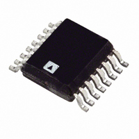
ADT7518ARQ-REEL Analog Devices Inc, ADT7518ARQ-REEL Datasheet - Page 4

ADT7518ARQ-REEL
Manufacturer Part Number
ADT7518ARQ-REEL
Description
IC SENSOR TEMP W/ADC/DAC 16QSOP
Manufacturer
Analog Devices Inc
Datasheet
1.ADT7518ARQ.pdf
(40 pages)
Specifications of ADT7518ARQ-REEL
Rohs Status
RoHS non-compliant
Function
Temp Monitoring System (Sensor)
Topology
ADC, Comparator, Multiplexer, Register Bank
Sensor Type
External & Internal
Sensing Temperature
-40°C ~ 120°C, External Sensor
Output Type
I²C™, MICROWIRE™, QSPI™, SPI™
Output Alarm
No
Output Fan
No
Voltage - Supply
2.7 V ~ 5.5 V
Operating Temperature
-40°C ~ 120°C
Mounting Type
Surface Mount
Package / Case
16-QSOP
ADT7518
Parameter
CONVERSION TIMES
ROUND ROBIN UPDATE RATE
DAC EXTERNAL REFERENCE INPUT
ON-CHIP REFERENCE
OUTPUT CHARACTERISTICS
DIGITAL INPUTS
Slow ADC
Fast ADC
Slow ADC @ 25°C
Fast ADC @ 25°C
V
V
Reference Feedthrough
Channel-to-Channel Isolation
Reference Voltage
Temperature Coefficient
Output Voltage
DC Output Impedance
Short-Circuit Current
Power-Up Time
Input Current
V
V
Pin Capacitance
SCL, SDA Glitch Rejection
LDAC Pulse Width
REF
REF
IL
IH
, Input Low Voltage
Scale Factor
V
Internal Temperature
External Temperature
V
Internal Temperature
External Temperature
Averaging On
Averaging Off
Averaging On
Averaging Off
Averaging On
Averaging Off
Averaging On
Averaging Off
, Input High Voltage
DD
DD
Input Range
Input Impedance
/AIN
/AIN
1
4
7
4
4
4
5
4
Min
1
0.001
1.89
20
Typ
8.97
17.58
11.4
712
11.4
712
24.22
1.51
712
44.5
2.14
134
14.25
890
79.8
4.99
94.76
9.26
6.41
400.84
21.77
3.07
>10
–90
–75
2.25
80
0.5
25
16
2.5
5
3
Max
V
V
±1
0.8
10
50
DD
DD
Rev. A | Page 4 of 40
− 0.1
Unit
mV/°C
mV/°C
ms
µs
ms
µs
ms
ms
µs
µs
ms
µs
ms
µs
ms
ms
ms
ms
ms
µs
ms
ms
V
MΩ
dB
dB
V
ppm/°C
V
Ω
mA
mA
µs
µs
µA
V
V
pF
ns
ns
Conditions/Comments
0 V to V
0 V to 2 V
Single channel mode.
Averaging (16 samples) on.
Averaging off.
Averaging (16 samples) on.
Averaging off.
Averaging (16 samples) on.
Averaging off.
Averaging (16 samples) on.
Averaging off.
Averaging (16 samples) on.
Averaging off.
Averaging (16 samples) on.
Averaging off.
Time to complete one measurement cycle
through all channels.
AIN1 and AIN2 are selected on Pins 7 and 8.
AIN1 and AIN2 are selected on Pins 7 and 8.
D+ and D– are selected on Pins 7 and 8.
D+ and D– are selected on Pins 7 and 8.
AIN1 and AIN2 are selected on Pins 7 and 8.
AIN1 and AIN2 are selected on Pins 7 and 8.
D+ and D– are selected on Pins 7 and 8.
D+ and D– are selected on Pins 7 and 8.
Buffered reference.
Buffered reference and power-down mode.
Frequency = 10 kHz.
Frequency = 10 kHz.
This is a measure of the minimum and maximum
drive capability of the output amplifier.
V
V
Coming out of power-down mode. V
Coming out of power-down mode. V
V
All digital inputs.
Input filtering suppresses noise spikes of less
than 50 ns.
Edge triggered input.
DD
DD
IN
= 0 V to V
= 5 V.
= 3 V.
REF
REF
output. T
output. T
DD.
A
= –40°C to +120°C.
A
= –40°C to +120°C.
DD
DD
= 5 V.
= 3.3 V.


