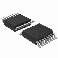
ADT7473ARQZ-REEL7 ON Semiconductor, ADT7473ARQZ-REEL7 Datasheet - Page 10

ADT7473ARQZ-REEL7
Manufacturer Part Number
ADT7473ARQZ-REEL7
Description
IC REMOTE THERMAL CTRLR 16QSOP
Manufacturer
ON Semiconductor
Series
dBCool®r
Datasheet
1.ADT7473ARQZ-1RL.pdf
(74 pages)
Specifications of ADT7473ARQZ-REEL7
Function
Fan Control, Temp Monitor
Topology
ADC, Comparator, Fan Speed Counter, Multiplexer, Register Bank
Sensor Type
External & Internal
Sensing Temperature
-40°C ~ 125°C, External Sensor
Output Type
SMBus™
Output Alarm
No
Output Fan
Yes
Voltage - Supply
3 V ~ 3.6 V
Operating Temperature
-40°C ~ 125°C
Mounting Type
Surface Mount
Package / Case
16-QSOP
Lead Free Status / RoHS Status
Lead free / RoHS Compliant
slave address allows the user to avoid conflicts with other
devices sharing the same serial bus, for example, if more
than one ADT7473−1 is used in a system.
pulses: eight bits of data followed by an acknowledge bit
from the slave device. Transitions on the data line must
occur during the low period of the clock signal and remain
stable during the high period because a low−to−high
transition when the clock is high might be interpreted as a
stop signal. The number of data bytes that can be transmitted
over the serial bus in a single read or write operation is
limited only by what the master and slave devices can
handle.
conditions are established. In write mode, the master pulls
the data line high during the tenth clock pulse to assert a stop
condition. In read mode, the master device overrides the
acknowledge bit by pulling the data line high during the low
period before the ninth clock pulse; this is known as No
Acknowledge. The master takes the data line low during the
low period before the tenth clock pulse, and then high during
the tenth clock pulse to assert a stop condition.
Figure 17. Writing a Register Address to the Address Pointer Register, then Writing Data to the Selected Register
The ability to make hardwired changes to the SMBus
Data is sent over the serial bus in sequences of nine clock
When all data bytes have been read or written, stop
Figure 16. Unpredictable SMBus Address if Pin 8
CARE SHOULD BE TAKEN TO ENSURE THAT PIN 8
(PWM3/ADDREN) IS EITHER TIED HIGH OR LOW. LEAVING PIN 8
FLOATING COULD CAUSE THE ADT7473-1 TO POWER UP WITH
AN UNEXPECTED ADDRESS.
NOTE THAT IF THE ADT7473-1 IS PLACED INTO ADDR SELECT
MODE, PINS 8 AND 4 CANNOT BE USED AS THE ALTERNATIVE
FUNCTIONS (PWM3, TACH4/THERM) UNLESS THE CORRECT
CIRCUIT IS MUXED IN AT THE CORRECT TIME OR DESIGNED TO
HANDLE THESE DUAL FUNCTIONS.
SDA
SCL
START BY
MASTER
ADT7473−1
PWM3/ADDREN
ADDR SELECT
1
0
is Unconnected
1
SERIAL BUS ADDRESS BYTE
4
8
DO NOT LEAVE ADDREN
UNCONNECTED! CAN
CAUSE UNPREDICTABLE
ADDRESSES.
0
V
CC
NC
10kΩ
1
FRAME 1
SDA (CONTINUED)
1
SCL (CONTINUED)
1
0
http://onsemi.com
ADT7473/ADT7473−1
R/W
ACK. BY
10
D7
9
1
serial bus in one operation, but it is not possible to mix read
and write in one operation, because the type of operation is
determined at the beginning and cannot subsequently be
changed without starting a new operation.
either one or two bytes, and read operations contain one
byte. To write data to one of the device data registers or read
data from it, the address pointer register must be set so the
correct data register is addressed, and then data can be
written into that register or read from it. The first byte of a
write operation always contains an address that is stored in
the address pointer register. If data is written to the device,
the write operation contains a second data byte that is written
to the register selected by the address pointer register.
address is sent over the bus, and then R/W is set to 0. This
is followed by two data bytes. The first data byte is the
address of the internal data register to be written to, which
is stored in the address pointer register. The second data byte
is the data to be written to the internal data register.
possibilities:
•
•
D7
D6
Any number of bytes of data can be transferred over the
In the ADT7473/ADT7473−1, write operations contain
This write operation is shown in Figure 17. The device
When reading data from a register, there are two
1
If the ADT7473/ADT7473−1’s address pointer register
value is unknown or not the desired value, it must first
be set to the correct value before data can be read from
the desired data register. This is done by performing a
write to the ADT7473/ADT7473−1, but only the data
byte containing the register address is sent, because no
data is written to the register. This is shown in
Figure 18.
A read operation is then performed consisting of the
serial bus address, R/W bit set to 1, followed by the
data byte read from the data register. This is shown in
Figure 19.
If the address pointer register is known to be already at
the desired address, data can be read from the
corresponding data register without first writing to the
address pointer register, as shown in Figure 19.
D6
D5
ADDRESS POINTER REGISTER BYTE
D5
D4
DATA BYTE
FRAME 3
D4
D3
FRAME 2
D3
D2
D2
D1
ADT7473/ADT7473−1
D1
D0
ADT7473/ADT7473−1
ACK. BY
D0
9
ACK. BY
STOP BY
MASTER
9


