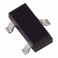
ADR510ART-R2 Analog Devices Inc, ADR510ART-R2 Datasheet - Page 8

ADR510ART-R2
Manufacturer Part Number
ADR510ART-R2
Description
IC REF SHUNT VOLT PREC 1V SOT-23
Manufacturer
Analog Devices Inc
Datasheet
1.ADR510ARTZ-REEL7.pdf
(12 pages)
Specifications of ADR510ART-R2
Rohs Status
RoHS non-compliant
Reference Type
Shunt
Voltage - Output
1V
Tolerance
±0.35%
Temperature Coefficient
70ppm/°C
Number Of Channels
1
Current - Cathode
100µA
Current - Output
10mA
Operating Temperature
-40°C ~ 85°C
Mounting Type
Surface Mount
Package / Case
SOT-23-3, TO-236-3, Micro3™, SSD3, SST3
Voltage - Input
-
Current - Quiescent
-
Other names
ADR510ART-R2TR
Available stocks
Company
Part Number
Manufacturer
Quantity
Price
Part Number:
ADR510ART-R2
Manufacturer:
ADI/亚德诺
Quantity:
20 000
ADR510
APPLICATIONS INFORMATION
The ADR510 is a 1.0 V precision shunt voltage reference
designed to operate without an external output capacitor
between the positive terminal and the negative terminal for
stability. An external capacitor can be used for additional
filtering of the supply.
As with all shunt voltage references, an external bias resistor
(R
(see Figure 2). R
through the load (I
supply voltage can vary, thus R
following conditions:
•
•
Given these conditions, R
voltage (V
ADR510, and the ADR510 output voltage.
ADJUSTABLE PRECISION VOLTAGE SOURCE
The ADR510, combined with a precision low input bias op amp
such as the AD860x, can be used to output a precise adjustable
voltage. Figure 11 illustrates implementation of this application
using the ADR510.
Output of the op amp, V
the circuit, which is completely dependent on the R2 and R1
resistors.
An additional capacitor in parallel with R2 can be added to
filter out high frequency noise. The value of C2 is dependent on
the value of R2.
BIAS
R
current to the ADR510 even when the supply voltage is at
minimum value and the load current is at maximum value.
R
exceed 10 mA when the supply voltage is at its maximum
value and the load current is at its minimum value.
V
R
) is required between the supply voltage and the ADR510
BIAS
BIAS
OUT
BIAS
ADR510
must be small enough to supply the minimum I
also needs to be large enough so that I
S
), the load and operating current (I
= 1
=
R
Figure 11. Adjustable Precision Voltage Source
BIAS
V
+
S
I
V
BIAS
L
CC
−
R2
R1
+
1.0V
R1
L
V
sets the current that is required to pass
) and the ADR510 (I
I
OUT
Q
OUT
BIAS
AD860x
(OPTIONAL)
, is determined by the gain of
is determined by the supply
R2
C2
BIAS
is chosen based on the
Q
V
). The load and the
OUT
= (1 + R2/R1)
L
and I
Q
does not
Q
) of the
Q
Rev. B | Page 8 of 12
(3)
(4)
OUTPUT VOLTAGE TRIM
Using a mechanical or digital potentiometer, the output voltage
of the ADR510 can be trimmed ±0.5%. The circuit in Figure 12
illustrates how the output voltage can be trimmed using a
10 kΩ potentiometer. Note that trimming using other resistor
values may not produce an accurate output from the ADR510.
USING THE ADR510 WITH PRECISION DATA
CONVERTERS
The compact ADR510 and its low minimum operating current
requirement make it ideal for use in battery-powered portable
instruments, such as the
use precision data converters.
Figure 13 shows the ADR510 serving as an external reference to
the AD7533, a CMOS multiplying DAC. Such a DAC requires a
negative voltage input in order to provide a positive output
range. In this application, the ADR510 is supplying a −1.0 V
reference to the REF input of the AD7533.
ADR510
Figure 13. ADR510 as a Reference for a 10-Bit CMOS DAC (AD7533)
R2
ADR510
–V
DD
+
–
R
V
BIAS
DD
Figure 12. Output Voltage Trim
MSB
V
1
2
G
CC
N
0
1
1
3
AD7533
3
2
470kΩ
R1
1
AD7533
CMOS multiplying DAC, that
15
9
LSB
POT
10kΩ
V
+
–
OUT
V
OUT
= 0V TO 1.0V


