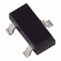
ADR510ART-R2 Analog Devices Inc, ADR510ART-R2 Datasheet

ADR510ART-R2
Specifications of ADR510ART-R2
Available stocks
Related parts for ADR510ART-R2
ADR510ART-R2 Summary of contents
Page 1
FEATURES Precision 1.000 V voltage reference Ultracompact 3 mm × SOT-23 package No external capacitor required Low output noise: 4 μV p-p (0 Hz) Initial accuracy: ±0.35% maximum Temperature coefficient: 70 ppm/°C maximum Operating current ...
Page 2
ADR510 TABLE OF CONTENTS Features .............................................................................................. 1 Applications....................................................................................... 1 Pin Configuration............................................................................. 1 General Description ......................................................................... 1 Revision History ............................................................................... 2 Specifications..................................................................................... 3 Electrical Characteristics............................................................. 3 Absolute Maximum Ratings............................................................ 4 Thermal Resistance ...................................................................... 4 ESD Caution.................................................................................. 4 Typical Performance Characteristics ............................................. ...
Page 3
SPECIFICATIONS ELECTRICAL CHARACTERISTICS I = 100 μ 25°C, unless otherwise noted Table 2. Parameter 1 Output Voltage Initial Accuracy Temperature Coefficient, A Grade Output Voltage Change vs Dynamic Output Impedance ...
Page 4
ADR510 ABSOLUTE MAXIMUM RATINGS Table 3. Parameter Reverse Current Forward Current Storage Temperature Range Operating Temperature Range Junction Temperature Range Lead Temperature (Soldering, 60 sec) Stresses above those listed under Absolute Maximum Ratings may cause permanent damage to the device. ...
Page 5
TYPICAL PERFORMANCE CHARACTERISTICS 1.002 1.001 1.000 0.999 0.998 0.997 TEMPERATURE (°C) Figure 3. Typical V vs. Temperature OUT V V OUT TIME (400ns/DIV) Figure 4. Turn-On Time V V OUT TIME (400µs/DIV) Figure 5. Turn-On ...
Page 6
ADR510 ΔI V OUT TIME (2µs/DIV) Figure 9. Output Response to 100 μA Input Current Change with 1 μF Capacitor = 100µ 50mV/DIV Rev Page 2µV/DIV TIME (400ms/DIV) Figure 10 ...
Page 7
PARAMETER DEFINITIONS TEMPERATURE COEFFICIENT This is the change of output voltage with respect to the operating temperature changes, normalized by the output voltage at 25°C. This parameter is expressed in parts per million/degrees Celsius (ppm/°C) and can be determined with ...
Page 8
ADR510 APPLICATIONS INFORMATION The ADR510 is a 1.0 V precision shunt voltage reference designed to operate without an external output capacitor between the positive terminal and the negative terminal for stability. An external capacitor can be used for additional filtering ...
Page 9
PRECISE NEGATIVE VOLTAGE REFERENCE The ADR510 is suitable for use in applications where a precise negative voltage reference is desired, including the application detailed in Figure 13. Figure 14 shows the ADR510 configured to provide an output of −1.0 V. ...
Page 10
... ADR510 OUTLINE DIMENSIONS ORDERING GUIDE Output Voltage Model (V ) Initial Accuracy OUT ADR510ART-REEL7 1.0 V 3.5 mV ADR510ART-R2 1 ADR510ARTZ-REEL7 1 ADR510ARTZ-R2 1 RoHS Compliant Part. # denotes lead free, may be top or bottom marked. 3.04 2.90 2.80 1.40 1.30 1.20 3 2.64 2.10 ...
Page 11
NOTES Rev Page ADR510 ...
Page 12
ADR510 NOTES ©2003–2007 Analog Devices, Inc. All rights reserved. Trademarks and registered trademarks are the property of their respective owners. D03270-0-9/07(B) Rev Page ...


