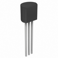
LT1123CZ#TR Linear Technology, LT1123CZ#TR Datasheet - Page 3

LT1123CZ#TR
Manufacturer Part Number
LT1123CZ#TR
Description
IC LDO REG DRIVER 5V TO-92-3
Manufacturer
Linear Technology
Type
Positive Fixedr
Datasheet
1.LT1123CZ.pdf
(16 pages)
Specifications of LT1123CZ#TR
Number Of Outputs
1
Voltage - Output
5V
Current - Supply
700µA
Operating Temperature
0°C ~ 125°C
Package / Case
TO-92-3 (Standard Body), TO-226
Lead Free Status / RoHS Status
Contains lead / RoHS non-compliant
Voltage - Input
-
Available stocks
Company
Part Number
Manufacturer
Quantity
Price
TYPICAL PERFOR
Drive Pin: The drive pin serves two functions. It provides
current to the LT1123 for its internal circuitry including
start-up, bias, current limit, thermal limit and a portion of
the base drive current for the output Darlington. The sum
total of these currents (450µA typical) is equal to the
minimum drive current. This current is listed in the speci-
fications as Drive Current with V
minimum current required by the drive pin of the LT1123.
The second function of the drive pin is to sink the base
drive current of the external PNP pass transistor. The
available drive current is specified for two conditions.
PI FU CTIO S
400
300
200
100
500
400
300
200
100
U
0
Feedback Pin Bias Current
vs Temperature
0
Feedback Pin Bias Current
vs Feedback Pin Voltage
0
V
FB
= 5V
25
U
1
FEEDBACK PIN VOLTAGE (V)
TEMPERATURE (°C)
T
J
50
= 25°C
2
U
T
75
J
3
= 125°C
T
W
100
J
= 0°C
4
LT1123 G01
LT1123 G04
A
U
125
FB
5
CE
= 5.2V. This is the
C
600
400
300
200
500
100
1.5
HARA TERISTICS
2.5
2.0
1.0
0.5
0
0
0
0
Drive Pin Saturation Voltage
vs Drive Current
Minimum Drive Pin Current
vs Temperature
V
V
DRIVE
FB
20
= 4.5V
25
= 3V
C
T
J
40
DRIVE CURRENT (mA)
TEMPERATURE (°C)
= 25°C
T
J
50
= 0°C
60
T
J
Drive current with V
available under nominal operating conditions, when the
device is regulating. Drive current with V
range of drive current available with the feedback pin
pulled low as it would be during start-up or during a short-
circuit fault. The drive current available when the feedback
pin is pulled low is less than the drive current available
when the device is regulating (V
in the curve of Drive Current vs V
Performance Characteristics curves. This can provide
some foldback in the current limit of the regulator circuit.
= 125°C
80
75
100
100
120
LT1123 G02
LT1123 G05
125
140
FB
5.03
5.02
4.97
5.01
5.00
4.99
4.98
= 4.80V gives the range of current
200
150
100
50
0
–50
Drive Current
vs Feedback Pin Voltage
0
Output Voltage vs Temperature
T
V
J
DRIVE
–25
= 25°C
1
FB
FEEDBACK PIN VOLTAGE (V)
= 3V
FB
= 5V). This can be seen
0
TEMPERATURE (°C)
Voltage in the Typical
2
25
FB
T
J
3
= –50°C
= 0.5V gives the
50
T
J
= 125°C
LT1123
4
75
100
5
LT1123 G03
LT1123 G06
1123fb
3
125
6


