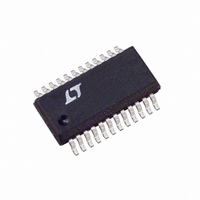
LTC3722EGN-2 Linear Technology, LTC3722EGN-2 Datasheet - Page 15

LTC3722EGN-2
Manufacturer Part Number
LTC3722EGN-2
Description
IC CTRLR PWM VOLTAGE-MODE 24SSOP
Manufacturer
Linear Technology
Datasheet
1.LTC3722EGN-1PBF.pdf
(28 pages)
Specifications of LTC3722EGN-2
Pwm Type
Voltage Mode, Full Bridge
Number Of Outputs
1
Frequency - Max
1MHz
Duty Cycle
98.5%
Voltage - Supply
3.8 V ~ 10.3 V
Buck
No
Boost
No
Flyback
No
Inverting
No
Doubler
No
Divider
Yes
Cuk
No
Isolated
Yes
Operating Temperature
-40°C ~ 85°C
Package / Case
24-SSOP
Frequency-max
1MHz
Lead Free Status / RoHS Status
Contains lead / RoHS non-compliant
Available stocks
Company
Part Number
Manufacturer
Quantity
Price
Part Number:
LTC3722EGN-2
Manufacturer:
LINEAR/凌特
Quantity:
20 000
operaTion
Fixed Delay Mode
The LTC3722-1/LTC3722-2 provides the flexibility through
the SBUS pin to disable the DirectSense delay circuitry
and enable fixed ZVS delays. The level of fixed ZVS delay
is proportional to the voltage programmed through the
voltage divider on the PDLY and ADLY pins (see Figure 3
for more detail).
Programming Adaptive Delay Time-Out
The LTC3722-1/LTC3722-2 controllers include a feature to
program the maximum time delay before a bridge switch
turn on command is summoned. This function will come
into play if there is not enough energy to commutate a
bridge leg to the opposite supply rail, therefore bypass-
ing the adaptive delay circuitry. The time delay can be
set with an external resistor connected between DPRG
and V
on DPRG is 2V. The external resistor programs a current
which flows into DPRG. The delay can be adjusted from
approximately 35ns to 300ns, depending on the resistor
value. If DPRG is left open, the delay time is approximately
400ns. The amount of delay can also be modulated based
on an external current source that feeds current into DPRG.
Care must be taken to limit the current fed into DPRG to
350µA or less.
R
DPRG
REF
(see Figure 4). The nominal regulated voltage
DPRG
V
REF
Figure 3. Setup for Fixed ZVS Delays
Figure 4. Delay Timeout Circuitry
V
SBUS
+
–
PDLY
ADLY
V
REF
2V
SBUS
R1
R2
R3
+
–
372212 F03
TURN-ON
OUTPUT
372212 F04
Powering the LTC3722-1/LTC3722-2
The LTC3722-1/LTC3722-2 utilize an integrated V
regulator to serve the dual purposes of limiting the volt-
age applied to V
voltage is sufficient to begin switching operation (under-
voltage lockout). With its typical 10.2V turn-on voltage
and 4.2V UVLO hysteresis, the LTC3722-1/LTC3722-2
is tolerant of loosely regulated input sources such as an
auxiliary transformer winding. The V
of sinking up to 25mA of externally applied current. The
UVLO turn-on and turn-off thresholds are derived from
an internally trimmed reference making them extremely
accurate. In addition, the LTC3722-1/LTC3722-2 exhibits
very low (145µA typ) start-up current that allows the use
of 1/8W to 1/4W trickle charge start-up resistors.
The trickle charge resistor should be selected as follows:
Adding a small safety margin and choosing standard
values yields:
APPLICATION
DC/DC
Off-Line
PFC Preregulator
V
ceramic capacitor to decouple the fast transient currents
demanded by the output drivers and a bulk tantalum or
electrolytic capacitor to hold up the V
the bootstrap winding, or an auxiliary regulator circuit
takes over.
CC
R
C
(minimum UVLO h h ysteresis)
HOLDUP
START MAX
should be bypassed with a 0.1µF to 1µF multilayer
(
LTC3722-1/LTC3722-2
=
CC
)
(
I
=
CC
as well as signaling that the chip’s bias
V
+
IN MIN
85V to 270V
I
(
DRIVE
36V TO 72V
V
IN
390V
)
RANGE
−
) •
DC
250
10 7
RMS
t
.
DELAY
. 3 8
µA
V
CC
V
CC
shunt is capable
supply before
R
1.4M
100k
430k
START
CC
shunt
372212fa


