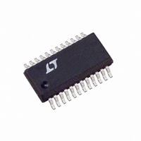
LTC3722EGN-2#TR Linear Technology, LTC3722EGN-2#TR Datasheet - Page 17

LTC3722EGN-2#TR
Manufacturer Part Number
LTC3722EGN-2#TR
Description
IC CTRLR PWM VOLTAGE-MODE 24SSOP
Manufacturer
Linear Technology
Datasheet
1.LTC3722EGN-1PBF.pdf
(28 pages)
Specifications of LTC3722EGN-2#TR
Pwm Type
Voltage Mode, Full Bridge
Number Of Outputs
1
Frequency - Max
1MHz
Duty Cycle
98.5%
Voltage - Supply
3.8 V ~ 10.3 V
Buck
No
Boost
No
Flyback
No
Inverting
No
Doubler
No
Divider
Yes
Cuk
No
Isolated
Yes
Operating Temperature
-40°C ~ 85°C
Package / Case
24-SSOP
Frequency-max
1MHz
Lead Free Status / RoHS Status
Contains lead / RoHS non-compliant
Available stocks
Company
Part Number
Manufacturer
Quantity
Price
operaTion
is designed so that the positive voltage square wave is
produced while the output inductor is freewheeling. An
advantage of this technique over the previous is that it
does not require a separate filter inductor and since the
voltage is derived from the well regulated output voltage, it
is also well controlled. One disadvantage is that this wind-
ing will require the same safety isolation that is required
for the main transformer. Another disadvantage is that a
much larger V
not generate a voltage as the output is first starting up,
or during short-circuit conditions.
Programming the LTC3722-1/LTC3722-2 Oscillator
The high accuracy LTC3722-1/LTC3722-2 oscillator circuit
provides flexibility to program the switching frequency,
slope compensation, and synchronization with minimal
external components. The LTC3722-1/LTC3722-2 oscillator
circuitry produces a 2.2V peak-to-peak amplitude ramp
waveform on C
used to synchronize other PWM chips. Typical maximum
duty cycles of 98.5% are obtained at 300kHz and 96% at
1MHz. A compensating slope current is derived from the
oscillator ramp waveform and sourced out of CS.
The desired amount of slope compensation is selected
with single external resistor. A capacitor to GND on C
programs the switching frequency. The C
current is internally set to a high value (>10mA). The dedi-
cated SYNC I/O pin easily achieves synchronization. The
C
1.25 C
T
OF SLAVE(S) IS
C
T
C
T
T
OF MASTER.
MASTER
LTC3722
Figure 8a. SYNC Output (Master Mode)
CC
T
SYNC
and a narrow pulse on SYNC that can be
filter capacitor is needed, since it does
5.1k
5 SLAVES
UP TO
•
•
•
1k
1k
5.1k
SYNC
5.1k
SYNC
T
LTC3722
LTC3722
SLAVES
ramp discharge
372212 F08a
C
C
T
T
C
C
T
T
T
LTC3722-1/LTC3722-2 can be set up to either synchronize
other PWM chips or be synchronized by another chip or
external clock source. The 1.8V SYNC threshold allows the
LTC3722-1/LTC3722-2 to be synchronized directly from
all standard 3V and 5V logic families.
Design Procedure:
1. Choose C
2. The LTC3722-1/LTC3722-2 can either synchronize other
switching frequency selected must be consistent with
the power magnetics and output power level. In general,
increasing the switching frequency will decrease the
maximum achievable output power, due to limitations
of maximum duty cycle imposed by transformer core
reset and ZVS. Remember that the tranformer fre-
quency is one-half that of the oscillator.
Example: Desired f
C
value of 220pF . A 5% or better tolerance multilayer NPO
or X7R ceramic capacitor is recommended for best
performance.
PWMs, or be synchronized to an external frequency
source or PWM chip (see Figure 8 for details).
C
T
T
FREQUENCY
EXTERNAL
= 1/(13.4k • f
SOURCE
=
Figure 8b. SYNC Input from an External Source
(
13 4
LTC3722-1/LTC3722-2
T
.
for the desired oscillator frequency. The
k
1
•
OSC
f
OSC
OSC
) = 226pF , choose closest standard
AMPLITUDE > 1.8V
100ns < PW < 0.4/
1k
)
= 330kHz
5.1k
SYNC
LTC3722
C
T
372212 F08b
C
T
372212fa


