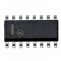
NCP1562BDR2G ON Semiconductor, NCP1562BDR2G Datasheet - Page 21

NCP1562BDR2G
Manufacturer Part Number
NCP1562BDR2G
Description
IC CLAMP/RESET PWM CTLR 16-SOIC
Manufacturer
ON Semiconductor
Datasheet
1.NCP1562ADBR2G.pdf
(26 pages)
Specifications of NCP1562BDR2G
Pwm Type
Voltage Mode
Number Of Outputs
2
Frequency - Max
1MHz
Duty Cycle
85%
Voltage - Supply
23.2 V ~ 100 V
Buck
No
Boost
Yes
Flyback
Yes
Inverting
Yes
Doubler
No
Divider
No
Cuk
No
Isolated
No
Operating Temperature
-40°C ~ 125°C
Package / Case
16-SOIC (3.9mm Width)
Frequency-max
1MHz
Topology
Flyback, Forward, Half-Bridge
Output Voltage
20 V
Output Current
2000 mA, 1000 mA
Switching Frequency
1000 KHz
Duty Cycle (max)
85 %
Maximum Operating Temperature
+ 125 C
Minimum Operating Temperature
- 40 C
Fall Time
10 ns
Mounting Style
SMD/SMT
Rise Time
26 ns
Synchronous Pin
Yes
Lead Free Status / RoHS Status
Lead free / RoHS Compliant
Other names
NCP1562BDR2G
NCP1562BDR2GOSTR
NCP1562BDR2GOSTR
Available stocks
Company
Part Number
Manufacturer
Quantity
Price
Company:
Part Number:
NCP1562BDR2G
Manufacturer:
ON Semiconductor
Quantity:
4 000
Part Number:
NCP1562BDR2G
Manufacturer:
ON/安森美
Quantity:
20 000
resistor, R
is proportional to R
obtained by grounding the t
trailing delay. This allows the user to optimize the delay for
the turn on transition of the main switch and ensures the
active clamp switch always exhibits zero volt switching.
Analog and Power Ground (PGND)
ground, PGND, terminal. GND is used for analog
connections such as V
others. PGND is used for high current connections such as
the internal output drivers. It is recommended to have
independent analog and power ground planes and connect
them at a single point, preferably at the ground terminal of
the system. This will prevent high current flowing on
PGND from injecting noise in GND. The PGND
connection should be as short and wide as possible to
reduce inductance- - induced spikes.
Oscillator
set by an R
A 500 mA current source (I
capacitor (C
(V
equation has two variables and can be solved iteratively. In
general, the time delay is a small portion of the ON time and
can be ignored as a first approximation. R
variation vs R
than 6.0 kΩ. Otherwise, the R
exceed the pulldown current and the oscillator will be in an
undefined state.
The output overlap delay is adjusted by connecting a
The leading delay is purposely made longer than the
The NCP1562 has an analog ground, GND, and a power
The oscillator frequency and maximum duty cycle are
The duty cycle, D, is given by Equation 7.
It can be observed that D is set by R
Figures 23 through 26 show the frequency and duty cycle
RTCT(peak)
D
T
, from the t
C
), typically 3.0 V. Once C
T
T
T
D =
) upon reaching its peak threshold
for several C
divider from V
t RTCT(C) + t RTCT(D)
D
D
. A minimum delay of 20 ns is
t RTCT(C) --t D
REF
pin to ground. The overlap delay
D
t RTCT(D) = R T C T × ln
, R
T
RTCT
values. R
pin.
REF
f =
T
T
C
C
) discharges the timing
T
D =
as shown in Figure 48.
R T C T × ln
T
, feedforward among
charge current will
T
T
T
ln
reaches its valley
, C
should not be less
T
V RTCT(valley) - -V REF
is then selected
V RTCT(peak) - -V REF
T
and t
V RTCT(valley) - -V REF
V RTCT(peak) - -V REF
D
ln
http://onsemi.com
(eq. 7)
. This
(I RTCT × R T ) + V RTCT(valley) --V REF
(I RTCT × R T ) + V RTCT(peak) --V REF
V RTCT(valley) - -V REF
V RTCT(peak) - -V REF
×
21
(I RTCT ×R T )+V RTCT(valley) - -V REF
(I RTCT ×R T )+V RTCT(peak) - -V REF
1
×
voltage (V
allowing C
waveform on the RTCT pin has a sawtooth like shape.
by OUT1 delayed by the overlap delay. Once V
is reached, OUT1 goes low, followed by OUT2 delayed by
t
overlap delay over the total charge and discharge (t
times. The charge and discharge times are calculated using
Equations 5 and 6. However, these equations are an
approximation as they do not take into account the
propagation delays of the internal comparator.
algebraic manipulation and replacing values, it simplifies
to:
to achieve a given duty cycle. Once the R
is chosen to obtain the desired operating frequency using
Equation 9.
Synchronization
architecture allows multiple NCP1562 to synchronize in a
master- - slave configuration. It can synchronize to
frequencies above or below the free running frequency.
D
(I RTCT ×R T )+V RTCT(valley) - -V REF
(I RTCT ×R T )+V RTCT(peak) - -V REF
OUT2 is set high once V
.
The duty cycle is the C
Substituting Equations 5, 6, and 7, and after a little
A proprietary bidirectional frequency synchronization
t RTCT(C) = R T C T × ln
--
R T C T
t D
Figure 48. Oscillator Configuration
RTCT(valley)
T
to charge back up through R
Enable
), typically 2.0 V, I
T
I
RTCT
charge time (t
RTCT(valley)
V RTCT(valley) --V REF
V RTCT(peak) --V REF
RTCT
V
REF
C
is reached, followed
R
T
T
RTCT(C)
T
RTCT
T
. The resulting
is selected, C
3 V
2 V
) minus the
turns OFF
RTCT(peak)
RTCT(D)
(eq. 5)
(eq. 9)
(eq. 6)
(eq. 8)
T
)


