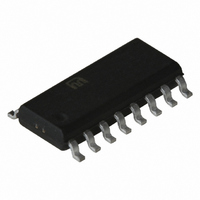
MIC2185BM Micrel Inc, MIC2185BM Datasheet - Page 10

MIC2185BM
Manufacturer Part Number
MIC2185BM
Description
IC CTRLR PWM SYNC BOOST 16-SOIC
Manufacturer
Micrel Inc
Datasheet
1.MIC2185YQS.pdf
(15 pages)
Specifications of MIC2185BM
Pwm Type
Current Mode
Number Of Outputs
1
Frequency - Max
440kHz
Duty Cycle
95%
Voltage - Supply
2.9 V ~ 14 V
Buck
No
Boost
Yes
Flyback
No
Inverting
No
Doubler
No
Divider
No
Cuk
No
Isolated
No
Operating Temperature
-40°C ~ 125°C
Package / Case
16-SOIC (3.9mm Width)
Frequency-max
440kHz
Lead Free Status / RoHS Status
Contains lead / RoHS non-compliant
PWM Operation
Figure 5 shows typical waveforms for PWM mode of operation.
The gate drive signal turns on the external low side MOSFET,
Q1, allowing the inductor current to ramp up. When the low
side MOSFET turns off and the high side MOSFET, Q2, turns
on, current flowing in the inductor forces the MOSFET drain
voltage to rise until the is clamped at approximately the output
voltage. The MIC2185 uses current mode control to improve
output regulation and simplify compensation of the control
loop. Current mode control senses both the output voltage
(outer loop) and the inductor current (inner loop). It uses the
inductor current and output voltage to determine the duty
cycle (D) of the buck converter. Sampling the inductor current
effectively removes the inductor from the control loop, which
simplifies compensation. A simplified current mode control
diagram is shown in figure 6.
A block diagram of the MIC2185 PWM current mode control
loop is shown in Figure 1. The inductor current is sensed by
measuring the voltage across a resistor, Rsense. The current
sense amplifier buffers and amplifies this signal. A ramp is
added to this signal to provide slope compensation, which is
MIC2185
(Low Side FE T Drain)
Switch NodeVoltage
V
V
IN
1A offset; 0.5A/di v
OUT
Inductor Current
High Side FET
RippleVoltage
Low Side FET
Gate Driver
Gate Drive
Gate Drive
200mV/div
Figure 5 - PWM mode waveforms
5V/div
5V/div
5V/div
Figure 6. PWM Control Loop
V
COMP
T
T
PER
ON
I_inductor
V
I_inductor
IN
= 3.3V
I_inductor
PWM ModeWaveform
I_inductor
V
OUT
= 5V
TIME (1µs/div)
Gate Drive at OUTN
I
OUT
= 0.75A
V
REF
Voltage
Divider
10
required in current mode control to prevent unstable operation
at duty cycles greater than 50%.
A transconductance amplifier is used as an error amplifier,
which compares an attenuated output voltage with a refer-
ence voltage. The output of the error amplifier is compared
to the current sense waveform in the PWM block. When the
current signal rises above the error voltage, the comparator
turns off the low side drive. The error signal is brought out to
the COMP pin (pin 4) allowing the use of external components
to stabilize the voltage loop.
Current Sensing and Overcurrent Protection
The inductor current is sensed during the switch on time by
a current sense resistor located between the source of the
MOSFET, Q1 and ground (R
the current limit threshold will immediately terminate the
gate drive of the N-channel MOSFET. This forces the Q1 to
operate at a reduced duty cycle, which reduces the output
voltage. In a boost converter, the overcurrent limit will
not protect the power supply or load during a severe
overcurrent condition or short circuit condition. If the
output is short-circuited to ground, current will flow from the
input, through the inductor and output diode,D1, to ground.
Only the impedance of the source and components limits
the current.
The minimum input voltage, maximum output power and
the minimum value of the current limit threshold determine
the value of the current sense resistor. The two switch, syn-
chronous operation of the MIC2185 forces the converter to
always operate in the continuous mode because current can
flow both ways through the high side P-channel MOSFET.
The equations below will help to determine the current sense
resistor value.
Maximum Peak Current
The peak inductor current is equal to the average inductor
current plus one half of the peak to peak inductor current.
The peak inductor current is:
V
However, the voltage drop across the inductor winding
resistance and low side MOSFET on-resistance must be
accounted for at the lower input voltages that the MIC2185
can operate at:
L
may be approximated as V
where:
I
V
V
L is the value of the boost inductor
f
η is the efficiency of the boost converter
V
I
I
IND(pk)
IND(pk)
O
S
O
IN
L
is the switching frequency
is the maximum output current
is the voltage across the inductor
is the output voltage
is the minimum input voltage
=
=
I
V
IND(ave)
V
O
IN
×
×
I
η
O
+
+
1
2
V
L
×
×
2 V
I
IND(pp)
×
(
SENSE
V
O
IN
O
−
×
(
for higher input voltage.
V
fs L
in Figure 1). Exceeding
IN
×
×
η
)
)
October 2005


