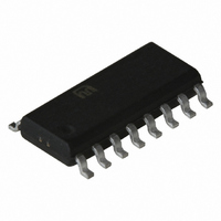
MIC2185BM Micrel Inc, MIC2185BM Datasheet - Page 9

MIC2185BM
Manufacturer Part Number
MIC2185BM
Description
IC CTRLR PWM SYNC BOOST 16-SOIC
Manufacturer
Micrel Inc
Datasheet
1.MIC2185YQS.pdf
(15 pages)
Specifications of MIC2185BM
Pwm Type
Current Mode
Number Of Outputs
1
Frequency - Max
440kHz
Duty Cycle
95%
Voltage - Supply
2.9 V ~ 14 V
Buck
No
Boost
Yes
Flyback
No
Inverting
No
Doubler
No
Divider
No
Cuk
No
Isolated
No
Operating Temperature
-40°C ~ 125°C
Package / Case
16-SOIC (3.9mm Width)
Frequency-max
440kHz
Lead Free Status / RoHS Status
Contains lead / RoHS non-compliant
during the discontinuous mode of operation found in lightly
loaded, non-synchronous boost converters. Pulling the SKIP
pin (pin 2) low will force the controller to operate in PWM
mode for all load conditions. Pulling the SKIP pin high will
force the controller to operate in SKIP mode.
Skip Mode Operation
This control method is used to improve efficiency at low output
loads. A block diagram of the MIC2185 skip mode is shown
in Figure 2. The power drawn by the MIC2185 control IC is
(I
IC can be a significant portion of the total output power during
periods of low output current, which lowers the efficiency of
the power supply. In skip mode the MIC2185 lowers the IC
supply current by disabling the high side drive and running
at lower than the PWM switching frequency. It also turns off
portions of the control and drive circuitry when the IC is not
switching. The disadvantage of this method is greater output
ripple and variable switching frequency. The Soft Start and
Sync pins have no effect when operating in skip mode.
In skip mode, switching starts when the feedback voltage
drops below the lower threshold level of the hysteresis com-
parator. The OutN pin goes high, turning on the N-channel
MOSFET, Q1. Current ramps up in the inductor until either
the SKIP mode current limit comparator or the hysteretic
voltage comparator turns off Q1’s gate drive. If the feedback
voltage exceeds the upper hysteretic threshold, Q1’s gate
drive is terminated. Or, if the voltage at the CSH pin exceeds
the skip mode current limit threshold, it terminates the gate
drive for that switching cycle. The gate drive remains off for
a constant period at the end of each switching cycle. This
off time period is typically 1us when the F/2 pin is low and
2us when the F/2 pin is high. Figure 3 shows some typical
switching waveforms in SKIP mode.
The skip mode current threshold limits the peak inductor
current per cycle. Depending on the input, output and circuit
parameters, many switching cycles can occur before the
feedback voltage exceeds the upper hysteretic threshold.
October 2005
VINA
(Low Side FE T Drain)
Switch NodeVoltage
V
OUT
· V
Inductor Current
RippleVoltage
Low Side FET
VINA
Gate Drive
200mV/div
5V/div
5V/div
5A/div
Figure 3. SKIP mode waveforms
) + (I
VINP
· V
VINP
). The power dissipated by the
SKIP Mode Waveform
TIME (50µs/div)
V
V
IN
OUT
= 3.3V
= 9V I
OUT
= 0.55A
9
Once the voltage on the feedback pin exceeds the upper
hysteretic threshold the gate drive is disabled. The output
load discharges the output capacitance causing Vout to
decrease until the feedback voltage drops below the lower
threshold voltage limit. The switching converter then turns
the gate drive back on. While the gate drive is disabled, the
MIC2185 draws less IC supply current then while it is switch-
ing, thereby improving efficiency at low output loads.
Figure 4 shows the improvement in efficiency that SKIP mode
makes when at lower output currents.
The maximum peak inductor current depends on the skip
current limit threshold and the value of the current sense
resistor, R
in skip mode, the peak inductor current is:
The maximum output current in skip mode depends on the
input conditions, output conditions and circuit component
values. Assuming a discontinuous mode where the inductor
current starts from zero at each cycle, the maximum output
current is calculated below:
where: I
I
I
V
V
L is the value of the boost inductor
f
η is the efficiency of the boost converter
R
2.5·10
current threshold (50mV)
INDUCTOR_pk
O(max)
S
O
IN
SENSE
O(max)
is the switching frequency
is the output voltage
is the input voltage
SENSE
=
-3
2 R
is the value of the current sense resistor
is a constant based on the skip mode
is the maximum output current
×
. For a typical 50mV current limit threshold
100
80
60
40
20
0
SENSE
=
2.5 10
R
50mV
Skip Mode Efficienc y
SENSE
OUTPUT CURRENT (A)
×
MIC2185 PWM vs.
2
Figure 4.
×
−
(
3
V
O
× ×
2
L fs
−
(
η
V
V
IN
OUT
P W M
400kHz
×
S K I P
=3.3V
V
=5V
IN
)
)
MIC2185


