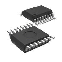
MIC2185BQS Micrel Inc, MIC2185BQS Datasheet - Page 7

MIC2185BQS
Manufacturer Part Number
MIC2185BQS
Description
IC CTRLR PWM SYNC BOOST 16-QSOP
Manufacturer
Micrel Inc
Datasheet
1.MIC2185YQS.pdf
(15 pages)
Specifications of MIC2185BQS
Pwm Type
Current Mode
Number Of Outputs
1
Frequency - Max
440kHz
Duty Cycle
95%
Voltage - Supply
2.9 V ~ 14 V
Buck
No
Boost
Yes
Flyback
No
Inverting
No
Doubler
No
Divider
No
Cuk
No
Isolated
No
Operating Temperature
-40°C ~ 125°C
Package / Case
16-QSOP
Frequency-max
440kHz
Lead Free Status / RoHS Status
Contains lead / RoHS non-compliant
Functional Diagram
Functional Description
The MIC2185 is a BiCMOS, switched mode, synchronous
boost (step up) control IC. The synchronous switched, high
side P-channel MOSFET, Q2, placed in parallel with the out-
put diode, D1, improves the efficiency of the boost converter.
The lower voltage drop across the MOSFET reduces power
dissipation and increases efficiency. Current mode control is
used to achieve superior transient line and load regulation.
An internal corrective ramp provides slope compensation
for stable operation above a 50% duty cycle. The controller
is optimized for high efficiency, high performance DC-DC
converter applications.
Figure 1 is a block diagram of the MIC2185 configured as
a PWM synchronous boost converter. The switching cycle
October 2005
V
IN
EN/UVLO
FREQ/2
COMP
SYNC
VREF
SKIP
VDD
SS
15
11
10
7
2
3
4
8
fs/4
Osc
Correction
Ramp
V
V
REF
DD
Control
Figure 1. MIC2185 PWM Mode Block Diagram
100k
Amplifier
C
Error
DECOUP
gm = 0.0002
Overcurrent Reset
PWM
Comparator
Gain = 20
SGND
S
On
GND
5
Bias
1
fs/4
V
V
IN
REF
A
Gain = 3.7
7
Frequency
Foldback
starts when OutN goes high and turns on the low side, N-
channel MOSFET, Q1. The Vgs of the MOSFET is equal to
VinP. This forces current to ramp up in the inductor. The
inductor current flows through the current sense resistor,
Rsense. The voltage across the resistor is amplified and
combined with an internal ramp for stability. This signal is
compared with the comp output signal of the error amplifier.
When the current signal equals the error voltage signal, the
low side MOSFET is turned off. The inductor current then
flows through the diode, D1, to the output. A delay between
the turn-off of the low side MOSFET and the turn-on of the
high side MOSFET prevents both MOSFETs from being on
at the same time, which would short the output to ground.
At the end of the non-overlap time, OutP pulls the gate of
the MOSFET to ground, turning on the high side, P-channel
V
V
REF
DD
Overcurrent
Comparator
0.1V
0.3V
C
IN
P
GND
P
P
GND
GND
V
16
OUTP
OUTN
CSH
9
PGND
12
FB
6
14
13
IN
P
Q1
L1
R
SENSE
D1
Q2
C
OUT
R1
R2
V
OUT
MIC2185


