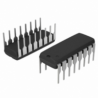
MC44605P ON Semiconductor, MC44605P Datasheet

MC44605P
Specifications of MC44605P
Available stocks
Related parts for MC44605P
MC44605P Summary of contents
Page 1
... Detection Current Sense Input 7 Demagnetization 8 Detection Input (Top View) *Winding Short Circuit Detection ORDERING INFORMATION Device Package MC44605PG PDIP−16 (Pb−Free) 1 MARKING DIAGRAM 16 MC44605P AWLYYWWG ref 15 WSCD* Program 14 Voltage Feedback Input Error Amp Output 13 12 Disabling Block (C ) ext 11 Soft-Start Input 10 Osc Capacitor (C ...
Page 2
Demagnetization Demagnetization Detection Input 8 Management V DT Output Synchronization 9 and EHTOVP Input Sf W.S.C.D* Comparator E.H.T.OVP Block WSCD C ext Disabling 12 Block Dis out V ref + Error Voltage AMP 14 ...
Page 3
MAXIMUM RATINGS Rating Total Power Supply and Zener Current Output Supply Voltage with Respect to Ground Output Current Source Sink Output Energy (Capacitive Load per Cycle) Soft−Start Current Sense, Voltage Feedback, E/A Output, C E.H.T.OVP, Sync Input Current Source Sink ...
Page 4
ELECTRICAL CHARACTERISTICS min/max values T = −25° to +85°C unless otherwise noted.) (Note 4) A Characteristic ERROR AMPLIFIER SECTION Voltage Feedback Input (V = 2.5 V) E/A out Input Bias Current ( Open Loop Voltage Gain ...
Page 5
ELECTRICAL CHARACTERISTICS min/max values T = −25° to +85°C unless otherwise noted.) (Note 5) A Characteristic REFERENCE SECTION Reference Output Voltage ( Reference Current Range ( ref ref ref Reference ...
Page 6
ELECTRICAL CHARACTERISTICS min/max values T = −25° to +85°C unless otherwise noted.) (Note 14) A Characteristic DISABLING BLOCK SECTION Delay Pulse Width Ratio (EHTOVP and WSCD Disabling Capacitor Charge Current)I Ratio (MPL and OHD Disabling Capacitor Charge Current)I Minimum V ...
Page 7
Pin Name Output 4 GND 5 Maximum Power Limitation 6 Over−Heating Detection 7 Current Sense Input 8 Demagnetization Detection 9 Synchronization and E.H.T.OVP Input 10 Oscillator Capacitor Soft−Start 12 C ...
Page 8
The following table consists of equations enabling to dimension a multisynchronized SMPS operating in discontinuous mode. Pout max Pin max + η 2 ·Vac NVo min 2 ·Vac )NVo min Lp max + 2 Pin max fsync max 2 Pin ...
Page 9
The Error Amp Output (Pin 13) is provided for external loop compensation. The output voltage is offset by two diodes drops ([1.4 V) and divided by three before it connects to the inverting input of the Current Sense Comparator. This ...
Page 10
V (maximum value of V disable 1 hysteresis is 4 13.6 V]. stup−th min The large hysteresis and the low startup current of the MC44605 make it ideally suited for off−line converter applications where ...
Page 11
Inductor current V DT Oscillator V int Sf Output Synchro input Inductor current V DT Oscillator V int Sf Output a − Free mode b − Synchronized mode Figure 5b. Oscillator Behavior http://onsemi.com 11 ...
Page 12
In effect, the output of the latch L1 is: — high during the oscillator capacitor charge and during the REGUL phase — low for the oscillator capacitor discharge Now, the latch L2 is set when the L1 output is high ...
Page 13
V Synchro. CC Signal Negative Active Clamping System Pin 9 R −200 mV Figure 6. Synchronization Demagnetization Section This block is incorporated to detect the complete core demagnetization in order to prevent the power MOSFET from switching on if the ...
Page 14
V ref τ Delay 5 Out 2 Enable In C OVLO 2 ref the Output is Disabled) Figure 9. Overvoltage Protection A delay (2 ms) is incorporated in ...
Page 15
V )/R (Vin x dt/L CS shift Figure 12. Overcurrent in a WSCD Case Now, in normal working, this overcurrent DIpk is equal to: DIpk + Vin δ where: ...
Page 16
Vcs + R Ipk S So Γ MPL MPL V + MPL comparator is used to compare V MPL of which, Dis , is connected to the “definitive inhibition MPL latch” of the disabling ...
Page 17
Consequently, by replacing V OHD value) in the last equation, the value R deducted: 2.5 R ref R + OHD Γ OHD S where are the maximum on time losses on max acceptable. Disabling Block ...
Page 18
Vac to 264 Vac RFI R1 Filter ... D4 1N4007 47 kW/2W SYNC 3 470 1N4148 kW 13 ...
Page 19
Input Voltage Synchronization Range Outputs Measured Efficiency (Pout = 64 W) Standby Losses (No Load − Pout = 0) EHTovp Threshold Maximum Power Limitation Overheating Detection (Pout = 64 W): The input rms levels at which the circuit detects an ...
Page 20
... Opportunity/Affirmative Action Employer. This literature is subject to all applicable copyright laws and is not for resale in any manner. PUBLICATION ORDERING INFORMATION LITERATURE FULFILLMENT: Literature Distribution Center for ON Semiconductor P.O. Box 5163, Denver, Colorado 80217 USA Phone: 303−675−2175 or 800−344−3860 Toll Free USA/Canada Fax: 303− ...


