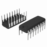
MC44605P ON Semiconductor, MC44605P Datasheet - Page 16

MC44605P
Manufacturer Part Number
MC44605P
Description
IC CTRLR PWM FREQ LATCH 16DIP
Manufacturer
ON Semiconductor
Series
GreenLine™r
Type
High Performance Latched Mode PWM Contollerr
Datasheet
1.MC44605P.pdf
(20 pages)
Specifications of MC44605P
Pwm Type
Current Mode
Number Of Outputs
1
Frequency - Max
250kHz
Duty Cycle
80%
Voltage - Supply
10 V ~ 15 V
Buck
No
Boost
No
Flyback
Yes
Inverting
No
Doubler
No
Divider
No
Cuk
No
Isolated
Yes
Operating Temperature
-25°C ~ 85°C
Package / Case
16-DIP (0.300", 7.62mm)
Frequency-max
250kHz
Output Voltage Range
2.4 V to 2.6 V
Input Voltage Range
+ 14.5 V to + 18 V
Mounting Style
Through Hole
Lead Free Status / RoHS Status
Contains lead / RoHS non-compliant
Other names
MC44605POS
Available stocks
Company
Part Number
Manufacturer
Quantity
Price
Part Number:
MC44605P
Manufacturer:
MOTOROLA/摩托罗拉
Quantity:
20 000
and:
So:
of which, Dis
latch” of the disabling block. So, when the calculated power
is higher than the threshold, the circuit is definitively
disabled (the system considers that there is an overload
condition).
the R
Overheating Detection Section (O.H.D.)
In the O.H.D. block, that is the power MOSFET heating
which is calculated, using the following equation:
where: p
A comparator is used to compare V
Finally, replacing V
In the MPL block, the converter input power is calculated.
V
MPL
MPL
R
d is the duty cycle
R
on
dson
value to be used, can be deducted:
MPL
+
are the power switch on−time losses
V
MPL
is the conduction MOSFET resistor
p on + 1
MPL
2
+
Figure 14. OHD and MPL
, is connected to the “definitive inhibition
Γ
R
T
MPL
k
2.5 V
2.5 V
MPL
Vcs + R
OHD
OHD
3
MPL
Output
Vcs
R
Vcs
by 2.5 V (the threshold value),
x
dson
C
Dis
2
Dis
Γ
Disabling
1.25
L
T
S
V
MPL
Block
P
OHD
MPL
MPL
MC44605
R 2
Ipk
Ipk 2
S
L
MPL
C
P
T
k
T
MPL
MPL
(Pin) max
to V
Sf
d
Vcs
R 2
ref
S
2
, the output
Pin
http://onsemi.com
16
by building a current source proportional to Vcs
on this current source of a “chopper” controlled by the
circuit output. By this means, the pin 6 average current is
proportional to the squared peak current multiplied to the
duty cycle (refer to Figure 14).
(R
the conduction losses can be obtained.
2.5 V. If V
block is activated by Dis
calculated V
are equal to their maximum value.
In effect,
where: k
source I
where: k2 is a constant
So:
Finally:
where: Γ
Now, as:
So, replacing Vcs and using the p
corresponding to V
dissipation is such that the heating is higher than this
threshold, the “definitive inhibition latch” of the Disabling
Block is activated and so, the output gets definitively
disabled.
As in the MPL section, the squared Ipk term is estimated
The duty cycle is taken into account thanks to the action
So, using an external resistor and capacitor network
Like in the MPL block, this voltage V
The external resistor R
Now, as k
So, by choosing the value of R
OHD
, C
specification. This is a constant equal to k2.
ref
OHD
OHD
OHD
V
OHD
, is proportional to 1/R
V
OHD
V
V
OHD
OHD
OHD
OHD
OHD
is the multiplier gain
) on this pin, a voltage V
is the OHD parameter as defined in the
gets higher than this threshold, the disabling
+ R
that is depending on the reference current
equal to 2.5 V when the conduction losses
+
+ R
+
k
3
OHD
Vcs + R
ref
OHD
R
OHD
OHD
OHD
is determined. If the MOSFET
R
OHD
+ k2
OHD
R
ref
(output of the comparator).
k
S
OHD
choice enables to obtain a
k2
Γ
ref
OHD
on
R
Ipk
R
R
Γ
:
ref
equation:
1
ref
OHD
dson
Vcs 2
R
OHD
OHD
Vcs 2
ref
OHD
Vcs 2
, proportional to
, is compared to
, the heating
R 2
d
S
d
2
.
d
p on


