LT1581CT7#PBF Linear Technology, LT1581CT7#PBF Datasheet - Page 5
LT1581CT7#PBF
Manufacturer Part Number
LT1581CT7#PBF
Description
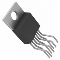
IC LDO REGULATOR 10A ADJ TO220-7
Manufacturer
Linear Technology
Datasheet
1.LT1581CT7PBF.pdf
(12 pages)
Specifications of LT1581CT7#PBF
Applications
Converter, Intel Pentium®
Voltage - Input
1.68 ~ 6 V
Number Of Outputs
1
Voltage - Output
1.25 ~ 4.65 V
Operating Temperature
0°C ~ 125°C
Mounting Type
Through Hole
Package / Case
TO-220-7 (Bent and Staggered Leads)
Primary Input Voltage
6V
Dropout Voltage Vdo
430mV
No. Of Pins
7
Output Current
10A
Operating Temperature Range
0°C To +125°C
Msl
MSL 1 - Unlimited
Termination Type
Through Hole
Rohs Compliant
Yes
Lead Free Status / RoHS Status
Lead free by exemption / RoHS Compliant
Available stocks
Company
Part Number
Manufacturer
Quantity
Price


BLOCK DIAGRA
APPLICATIONS
The LT1581 is a low dropout regulator designed to power
the new generation of microprocessors. Low dropout
regulators have become more common in desktop com-
puter systems as microprocessor manufacturers have
moved away from 5V only CPUs. A wide range of supply
requirements exists today with new voltages just over the
horizon. In many cases the input/output differential is very
small, effectively disqualifying many of the low dropout
regulators on the market today. The LT1581 is designed to
make use of multiple power supplies present in most
systems to reduce the dropout voltage. This 2-supply
approach maximizes efficiency.
The second supply, at least 1V greater than the output
voltage, is used to provide power for the control circuitry
and supply the drive current to the NPN output transistor.
This allows the NPN to be driven into saturation, thereby
reducing the dropout voltage by a V
conventional designs. The current requirement for the
U
INFORMATION
U
W
ADJ
W
BE
SENSE
GND
compared to
CONTROL
U
FOR FIXED
VOLTAGE
DEVICE
control voltage is relatively small, equal to approximately
1% of the output current or about 100mA for a 10A load.
The bulk of this current is drive current for the NPN output
transistor. This drive current becomes part of the output
current.
The control voltage must be at least 1V greater than the
output voltage to obtain optimum performance. The maxi-
mum voltage on the V
voltage at the V
for fixed voltage devices is 6mA (typ) and is constant as a
function of load. ADJUST pin current for adjustable de-
vices is 60 A at 25 C and varies proportional to absolute
temperature.
The LT1581 has improved frequency compensation which
permits the use of capacitors with very low ESR. This is
critical in addressing the needs of modern, low voltage,
high speed microprocessors. Current generation micro-
+
–
POWER
pin is limited to 7V. GND pin current
CONTROL
LT1581/LT1581-2.5
pin is 13V. The maximum
OUTPUT
POWER
1581 BD
5
Related parts for LT1581CT7#PBF
Image
Part Number
Description
Manufacturer
Datasheet
Request
R

Part Number:
Description:
CD ROM LINEARVIEW DATASHEETS
Manufacturer:
Linear Technology

Part Number:
Description:
Standalone Linear Li-Ion Battery Charger with Thermal Regulation in ThinSOT
Manufacturer:
Linear Technology Corporation
Datasheet:
Part Number:
Description:
Low noise, high frequency, 8th order linear phase lowpass filter
Manufacturer:
Linear Technology Corporation
Datasheet:
Part Number:
Description:
Manufacturer:
Linear Technology Corporation
Datasheet:
Part Number:
Description:
Manufacturer:
Linear Technology Corporation
Datasheet:
Part Number:
Description:
Manufacturer:
Linear Technology Corporation
Datasheet:
Part Number:
Description:
Manufacturer:
Linear Technology Corporation
Datasheet:
Part Number:
Description:
Manufacturer:
Linear Technology Corporation
Datasheet:
Part Number:
Description:
Manufacturer:
Linear Technology Corporation
Datasheet:
Part Number:
Description:
Manufacturer:
Linear Technology Corporation
Datasheet:
Part Number:
Description:
Dual and Quad, JFET Input Precision High Speed Op Amps
Manufacturer:
Linear Technology Corporation
Datasheet:
Part Number:
Description:
Manufacturer:
Linear Technology Corporation
Datasheet:
Part Number:
Description:
1, 2, 6 and 8 Channel, 10-Bit Serial I/O Data Acquisition Systems
Manufacturer:
Linear Technology Corporation
Datasheet:
Part Number:
Description:
Manufacturer:
Linear Technology Corporation
Datasheet:
Part Number:
Description:
Universal dual filter building block
Manufacturer:
Linear Technology Corporation
Datasheet: