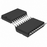
LTC1753CSW#TRPBF Linear Technology, LTC1753CSW#TRPBF Datasheet - Page 16

LTC1753CSW#TRPBF
Manufacturer Part Number
LTC1753CSW#TRPBF
Description
IC SW REG CNTRLR PENT III 20SOIC
Manufacturer
Linear Technology
Datasheet
1.LTC1753CGPBF.pdf
(24 pages)
Specifications of LTC1753CSW#TRPBF
Applications
Controller, Intel Pentium® III
Voltage - Input
5V
Number Of Outputs
1
Voltage - Output
1.3 ~ 3.5 V
Operating Temperature
0°C ~ 70°C
Mounting Type
Surface Mount
Package / Case
20-SOIC (7.5mm Width)
Lead Free Status / RoHS Status
Lead free / RoHS Compliant
Available stocks
Company
Part Number
Manufacturer
Quantity
Price
APPLICATIO S I FOR ATIO
LTC1753
Note that capacitor manufacturers’ ripple current ratings
are often based on only 2000 hours (three months)
lifetime at rated temperature. Further derating of the input
capacitor ripple current beyond the manufacturer’s speci-
fication is recommended to extend the useful life of the
circuit. Lower operating temperature will have the largest
effect on capacitor longevity.
The output capacitor in a buck converter sees much less
ripple current under steady-state conditions than the input
capacitor. Peak-to-peak current is equal to that in the
inductor, usually 10% to 40% of the total load current.
Output capacitor duty places a premium not on power
dissipation but on ESR. During an output load transient,
the output capacitor must supply all of the additional load
current demanded by the load until the LTC1753 can
adjust the inductor current to the new value. Output
capacitor ESR results in a step in the output voltage equal
to the ESR value multiplied by the change in load current.
An 11A load step with a 0.05 ESR output capacitor will
result in a 550mV output voltage shift; this is 19.6% of the
output voltage for a 2.8V supply! Because of the strong
relationship between output capacitor ESR and output
load transient response, the output capacitor is usually
chosen for ESR, not for capacitance value; a capacitor with
suitable ESR will usually have a larger capacitance value
than is needed for energy storage.
Electrolytic capacitors rated for use in switching power
supplies with specified ripple current ratings and ESR can
be used effectively in LTC1753 applications. OS-CON
electrolytic capacitors from Sanyo and other manufactur-
ers give excellent performance and have a very high
performance/size ratio for electrolytic capacitors. Surface
mount applications can use either electrolytic or dry
tantalum capacitors. Tantalum capacitors must be surge
tested and specified for use in switching power supplies.
Low cost, generic tantalums are known to have very short
lives followed by explosive deaths in switching power
supply applications. AVX TPS series surface mount
devices are popular surge tested tantalum capacitors that
work well in LTC1753 applications.
A common way to lower ESR and raise ripple current
capability is to parallel several capacitors. A typical LTC1753
application might exhibit 5A input ripple current. Sanyo
OS-CON part number 10SA220M (220 F/10V) capacitors
16
U
U
W
U
feature 2.3A allowable ripple current at 85 C; three in
parallel at the input (to withstand the input ripple current)
will meet the above requirements. Similarly, AVX
TPSE337M006R0100 (330 F/6V) have a rated maximum
ESR of 0.1 ; seven in parallel will lower the net output
capacitor ESR to 0.014 . For low cost application, Sanyo
MV-GX series of capacitors can be used with acceptable
performance. The small size, low profile Sanyo OS-CON
4SP820M comes with extremely low ESR (typically 0.008
at room temperature). This is an excellent choice for
output capacitor usage. However, due to the low ESR, it
requires attention to frequency compensation. Refer to
the Feedback Loop Compensation section for details.
Feedback Loop Compensation
The LTC1753 voltage feedback loop is compensated at the
COMP pin, attached to the output node of the internal g
error amplifier. The feedback loop can generally be com-
pensated properly with an RC + C network from COMP to
GND as shown in Figure 7a.
Loop stability is affected by the values of the inductor,
output capacitor, output capacitor ESR, FET R
amplifier transconductance and error amplifier compen-
sation network. The inductor and the output capacitor
create a double pole at the frequency:
f
R
LC
C
C
C
=
2
COMP
10
Figure 7a. Compensation Pin Hook-Up
(L
C1
O
1
)(C
LTC1753
OUT
)
ERR
–
+
1 F
DAC
6
R2
R1
1753 F07a
SENSE
DS(ON) ,
V
11
FB
error
1753fa
m
C2


