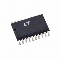
LTC1753CSW Linear Technology, LTC1753CSW Datasheet

LTC1753CSW
Specifications of LTC1753CSW
Available stocks
Related parts for LTC1753CSW
LTC1753CSW Summary of contents
Page 1
... SPARC, the PWM duty cycle can be momentarily forced 100% to reduce the output voltage recovery time. , LTC and LT are registered trademarks of Linear Technology Corporation. Pentium is a registered trademark of Intel Corporation. AMD- registered trademark of Advanced Micro Devices, Inc ...
Page 2
... OUTEN = 0, VID0 to VID4 Floating (Figure 12V, OUTEN = V (Note 6) (Figure 12V, OUTEN = 0, VID0 to VID4 Floating CC (Figure 4) (Note 11) (Note 11 TOP VIEW ORDER PART NUMBER OUTEN 18 VID0 LTC1753CG 17 VID1 LTC1753CSW 16 VID2 15 VID3 14 VID4 13 PWRGD 12 FAULT PACKAGE 20-LEAD PLASTIC SO = 100 100 C/ W (SW MIN TYP MAX 4 ...
Page 3
ELECTRICAL CHARACTERISTICS The denotes specifications which apply over the full operating temperature range, otherwise specifications are 5V 12V, unless otherwise noted. (Note SYMBOL PARAMETER G Error Amplifier Open-Loop DC Gain ERR ...
Page 4
LTC1753 W U TYPICAL PERFOR A CE CHARACTERISTICS Typical 1.3V V Distribution OUT 50 TOTAL SAMPLE SIZE = 500 100 1.275 1.285 1.295 1.305 1.315 OUTPUT VOLTAGE (V) 1753 G01 Load Regulation ...
Page 5
W U TYPICAL PERFOR A CE CHARACTERISTICS Oscillator Frequency vs Temperature 350 340 330 320 310 300 290 280 270 260 250 – 125 –25 100 TEMPERATURE ( C) 1753 G10 V Operating Supply Current CC ...
Page 6
LTC1753 W U TYPICAL PERFOR A CE CHARACTERISTICS Expanded View of Undershoot Illustrates 100% Duty Cycle Operation 2.8V OUT V OUT 20mV/DIV G1 10V/DIV 5 s/DIV CTIO S G2 (Pin 1): Gate Drive ...
Page 7
CTIO S COMP (Pin 10): External Compensation. The COMP pin is connected directly to the output of the error amplifier and the input of the PWM comparator network is used at ...
Page 8
LTC1753 W BLOCK DIAGRA + 113% V REF FC – OUTEN 19 COMP REF MHCL HCL MONO 8 12 FAULT DISDR LOGIC SYSTEM POWER DOWN – R PWM S + ERR ...
Page 9
TEST CIRCUITS 100pF 100pF VID0 TO VID4 15k 150pF C C 4700pF 0 SENSE OUT ...
Page 10
LTC1753 CTIO TABLES Table 1. PWRGD and FAULT Logic INPUT OUTEN V ** FAULT SENSE < 97% 1 > 97% < 103% 1 >103% 1 > 113% Table 2. Rated Output Voltage INPUT PIN ...
Page 11
U U APPLICATIO S I FOR ATIO conventional TTL enable signal. The free-running 300kHz PWM frequency can be synchronized to a faster external clock connected to OUTEN. Adjusting the oscillator fre- quency can add flexibility in the external component selection. ...
Page 12
LTC1753 U U APPLICATIO S I FOR ATIO Table 3. Recommended R Resistor ( Maximum Operating Load Current and External MOSFET Q1 IMAX MAXIMUM OPERATING LOAD CURRENT (A) Si4410 8 820 10 1.2k 12 — 14 — 16 ...
Page 13
U U APPLICATIO S I FOR ATIO mounted next to the external MOSFET which is expected to run the hottest –– often the high-side device, Q1. Elec- trically, the thermistor should form a voltage divider with another resistor, R1, connected ...
Page 14
LTC1753 U U APPLICATIO S I FOR ATIO The R required for a given conduction loss can now DS(ON) be calculated by rearranging the relation MAX ...
Page 15
U U APPLICATIO S I FOR ATIO in the R calculations will generally decrease MOSFET DS(ON) cost and circuit efficiency while increasing MOSFET heat sink requirements. Inductor Selection The inductor is often the largest component in the LTC1753 design and ...
Page 16
LTC1753 U U APPLICATIO S I FOR ATIO Note that capacitor manufacturers’ ripple current ratings are often based on only 2000 hours (three months) lifetime at rated temperature. Further derating of the input capacitor ripple current beyond the manufacturer’s speci- ...
Page 17
U U APPLICATIO S I FOR ATIO The ESR of the output capacitor forms a zero at the frequency ESR 2 (ESR)(C ) OUT The compensation network at the error amplifier output is to provide enough phase ...
Page 18
LTC1753 U U APPLICATIO S I FOR ATIO response using a network analyzer to find the actual loop poles and zeros. Table 5 shows the suggested compensation components for 5V input applications based on the inductor and output capacitor values. ...
Page 19
U U APPLICATIO S I FOR ATIO possible. It should also be located as close as possible above (or below) the power ground plane. Some of the phase shift problem can be solved by taking the AC feedback locally at ...
Page 20
LTC1753 U U APPLICATIO S I FOR ATIO LAYOUT CONSIDERATIONS When laying out the printed circuit board, the following checklist should be used to ensure proper operation of the LTC1753. These items are also illustrated graphically in the layout diagram ...
Page 21
U U APPLICATIO S I FOR ATIO OUT + + C OUT BOLD LINES INDICATE HIGH CURRENT PATHS = GROUND PLANE 0 ...
Page 22
LTC1753 PACKAGE DESCRIPTIO 5.20 – 5.38** (0.205 – 0.212) 0.13 – 0.22 0.55 – 0.95 (0.005 – 0.009) (0.022 – 0.037) NOTE: DIMENSIONS ARE IN MILLIMETERS * DIMENSIONS DO NOT INCLUDE MOLD FLASH. MOLD FLASH SHALL NOT EXCEED 0.152mm (0.006") ...
Page 23
... DIMENSION DOES NOT INCLUDE INTERLEAD FLASH. INTERLEAD FLASH SHALL NOT EXCEED 0.010" (0.254mm) PER SIDE Information furnished by Linear Technology Corporation is believed to be accurate and reliable. However, no responsibility is assumed for its use. Linear Technology Corporation makes no represen- tation that the interconnection of its circuits as described herein will not infringe on existing patent rights. ...
Page 24
... LTC1873 Dual 550kHz Synchronous 2-Phase Switching Regulator Controller with 5-Bit VID LTC1929 2-Phase, High Efficiency, Synchronous Step-Down Switching Regulator No R and PolyPhase are trademarks of Linear Technology Corporation. SENSE Linear Technology Corporation 24 1630 McCarthy Blvd., Milpitas, CA 95035-7417 (408) 432-1900 FAX: (408) 434-0507 + ...


