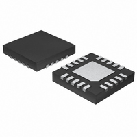
MAX1513ETP+T Maxim Integrated Products, MAX1513ETP+T Datasheet - Page 22

MAX1513ETP+T
Manufacturer Part Number
MAX1513ETP+T
Description
IC CNTRLR TFT-LCD PS 20-TQFN
Manufacturer
Maxim Integrated Products
Datasheet
1.MAX1513ETP.pdf
(28 pages)
Specifications of MAX1513ETP+T
Applications
Controller, TFT, LCD
Voltage - Input
2.7 ~ 5.5 V
Number Of Outputs
1
Voltage - Output
2.7 ~ 50 V
Operating Temperature
-40°C ~ 85°C
Mounting Type
Surface Mount
Package / Case
20-TQFN Exposed Pad
Lead Free Status / RoHS Status
Lead free / RoHS Compliant
TFT-LCD Power-Supply Controllers
The DC loop gain (A
where R1 and R2 are the feedback-divider resistors
(Figure 1), D is the duty cycle, I
tive maximum output current as described in the
Inductor Selection section, 0.554 is the gain of the cur-
rent-sense amplifier, and R
resistor value given by:
where R
and SF is either 1 or the scale factor in step 5 of the
Current-Sense Network Selection section.
The frequency of the dominant pole is:
The frequency of the RHP zero is:
The frequency of the ESR zero is:
The unity-gain crossover frequency is:
For stable operation, select an output capacitor with
enough capacitance and a low enough ESR to ensure
that the dominant pole is low enough so the loop gain
reaches unity well before either the ESR zero or the
RHP zero, the lower of which should preferably occur at
or above 5 times the unity-gain frequency as long as
the two zeros are well separated. Calculate the mini-
mum output capacitance for stable operation using:
If the RHP zero and the ESR zero occur simultaneously,
place the dominant pole so that the unity-gain frequen-
cy is less than 1/10th the frequency of the zeros.
Calculate the minimum output capacitance for stable
operation using:
22
C
A
OUT MIN
______________________________________________________________________________________
DC
f
Z RHP
f
P DOMINANT
(
(
f
L(TYP)
f
(
CROSSOVER
Z ESR
=
(
)
)
R
1
)
=
=
is the typical value of the inductor DCR,
R
+
=
R
2
(
2π
1
CS
R
-
2π
)
2
DC
×
D
=
×
=
=
)
×
) is approximately:
2
5
min
2π
A
0 554
SF
R
×
×
.
DC
[
ESR
f
CS
Z RHP
A
×
2
×
1
(
1
π
DC
×
I
-
V
MAIN EFF
R
is the equivalent sense-
×
×
MAIN
×
L TYP
D
f
MAIN(EFF)
P DOMINANT
(
×
)
R
C
(
,
L
f
CS
(
V
Z ESR
OUT
I
MAIN EFF
×
MAIN
(
)
×
I
×
MAIN EFF
)
C
)
(
I
]
OUT
MAIN EFF
×
is the effec-
V
(
MAIN
)
)
V
MAIN
(
)
)
where f
ESR zero.
Using the typical operating circuit in Figure 1 as an
example: the duty cycle is 0.67, the effective maximum
output current is 500mA, the inductor is 2.2µH with a
typical DCR of 24mΩ, and the output capacitor is 10µF
with a maximum ESR of 20mΩ. The scale factor for the
current-sense network is 1, so R
loop gain A
ESR zero is at 796kHz. Since the frequency of the ESR
zero is higher than that of the RHP zero, the unity-gain
crossover frequency should be determined based on
the RHP zero. The minimum output capacitance for sta-
ble operation is:
Lead or lag compensation can be useful to compen-
sate for particular component choices or to optimize
the transient response for various output capacitor or
inductor values.
Adding lead compensation (the R3/C1 network from
V
width, which can increase the speed of response to
transients. Too much speed can destabilize the loop
and is not needed or recommended for Figure 1’s com-
ponents. Lead compensation adds a zero-pole pair,
providing gain at higher frequencies and increasing
loop bandwidth. The frequencies of the zero and pole
for lead compensation depend on the feedback-divider
resistors and the RC network between V
The frequencies of the zero and pole for the lead com-
pensation are:
At high frequencies, R3 is effectively in parallel with R1,
determining the amount of added high-frequency gain.
If R3 is very large, there is no added gain and as R3
approaches zero, the added gain approaches the
inverse of the feedback-divider’s attenuation. A typical
value for R3 is greater than 1/2 of R1. The value of C1
MAIN
C
OUT MIN
f
f
to FB in Figure 11) increases the loop band-
Z LEAD
P LEAD
Z
C
_
_
OUT MIN
(
is the frequency of the RHP zero and the
DC
(
)
is 62, the RHP zero is at 236kHz, and the
=
=
=
)
2
2
2
=
π
5
π
π
10
×
×
×
×
236
(
⎛
⎜
⎝
2π
62
R
×
R
1
3
A
kHz
×
×
+
1
+
DC
500
R
f
Z
R
R
3
1
×
CS
×
1
1
)
×
mA
×
+
I
15
×
MAIN EFF
V
is 24mΩ. The DC
MAIN
R
R
V
C
2
2
1
(
⎞
⎟ ×
⎠
≈
MAIN
6 97
)
.
C
1
and FB.
µ
F


