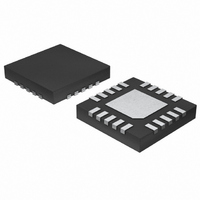
MAX1513ETP+T Maxim Integrated Products, MAX1513ETP+T Datasheet - Page 25

MAX1513ETP+T
Manufacturer Part Number
MAX1513ETP+T
Description
IC CNTRLR TFT-LCD PS 20-TQFN
Manufacturer
Maxim Integrated Products
Datasheet
1.MAX1513ETP.pdf
(28 pages)
Specifications of MAX1513ETP+T
Applications
Controller, TFT, LCD
Voltage - Input
2.7 ~ 5.5 V
Number Of Outputs
1
Voltage - Output
2.7 ~ 50 V
Operating Temperature
-40°C ~ 85°C
Mounting Type
Surface Mount
Package / Case
20-TQFN Exposed Pad
Lead Free Status / RoHS Status
Lead free / RoHS Compliant
capacitors, the output voltage ripple is dominated by
the capacitance value. Use the following equation to
approximate the required capacitor value:
where C
pump, I
pump, and V
output ripple.
The charge-pump output capacitor is typically also the
input capacitor for a linear regulator. Often, its value must
be increased to maintain the linear regulator’s stability.
Use low-cost silicon switching diodes with a current rating
equal to or greater than twice the average charge-pump
input current. If their low forward voltage helps to avoid an
extra stage, some or all of the diodes can be replaced
with Schottky diodes with equivalent current ratings.
Adjust the positive linear-regulator (REG P, REG L, and
REG G) output voltages by connecting a resistive volt-
age-divider from their respective outputs to the analog
ground plane (which connects to GND) with the center
tap connected to FB_ (Figure 1). Select the lower resis-
tor of the divider in the range of 10kΩ to 30kΩ. Calculate
the upper resistor with the following equation:
where V
ear regulator, and V
Adjust the gate-off linear-regulator REG N output volt-
age by connecting a resistive voltage-divider from
V
(Figure 1). Select R4 between 20kΩ and 50kΩ.
Calculate R3 with the following equation:
where V
only source up to 50µA; using a resistor less than 20kΩ
for R4 results in higher bias current than REF can sup-
ply without degrading REF accuracy.
GOFF
to REF with the center tap connected to FBN
OUT
FBN
OUT_CP
LOAD_CP
R
UPPER
C
_ is the output voltage of the respective lin-
= 250mV, V
RIPPLE_CP
R
OUT CP
3
=
is the output capacitor of the charge
_
______________________________________________________________________________________
=
Linear-Regulator Controllers
is the load current of the charge
R
FB
4
R
_ = 1.25V (typ).
LOWER
≥
×
Charge-Pump Rectifier Diodes
is the peak-to-peak value of the
REF
⎛
⎜
⎝
2
f
V
OSC RIPPLE CP
FBN
V
= 1.25V. Note that REF can
Output-Voltage Selection
REF
I
LOAD CP
×
V
TFT-LCD Power-Supply Controllers
-
⎛
⎜
⎝
-
V
V
V
V
_
OUT
GOFF
FBN
FB
_
_
_
⎞
⎟
⎠
- 1
⎞
⎟
⎠
The pass transistor must meet specifications for current
gain (h
tion voltage, and power dissipation. The transistor’s
current gain limits the guaranteed maximum output cur-
rent to:
where I
rent and R
the transistor’s base and emitter. Furthermore, the tran-
sistor’s current gain increases the linear regulator’s DC
loop gain (see the Stability Requirements section), so
excessive gain destabilizes the output. Therefore, tran-
sistors with current gain over 100 at the maximum out-
put current can be difficult to stabilize and are not
recommended unless needed to meet output-current
requirements.
The transistor’s saturation voltage at the maximum out-
put current determines the minimum input-to-output
voltage differential that the linear regulator supports.
Also, the package’s power dissipation limits the use-
able maximum power-dissipation capability of the tran-
sistor’s package, and mounting must exceed the actual
power dissipation in the device. The power dissipation
equals the maximum load current (I
times the maximum input-to-output voltage differential:
where V
linear regulator and V
the linear regulator.
The MAX1513/MAX1514 linear-regulator controllers use
an internal transconductance amplifier to drive an
external pass transistor. The transconductance amplifi-
er, the pass transistor, the base-emitter resistor, and
the output capacitor determine the loop stability. The
following applies equally to all linear regulators in the
MAX1513 and MAX1514.
The transconductance amplifier regulates the output
voltage by controlling the pass transistor’s base cur-
rent. The total DC loop gain is approximately:
P
=
FE
DRV
I
IN(MAX)_LR
LOAD MAX
I
LOAD MAX LR
), input capacitance, collector-emitter satura-
BE
is the minimum guaranteed base-drive cur-
(
is the pullup resistor connected between
(
)
)_
is the maximum input voltage of the
=
⎛
⎜
⎝
OUT_LR
I
DRV
×
(
V
Pass-Transistor Selection
-
IN MAX LR
R
V
(
is the output voltage of
BE
Stability Requirements
BE
⎞
⎟ ×
⎠
)_
h
LOAD(MAX)_LR
FE MIN
- V
(
OUT_LR
)
)
25
)


