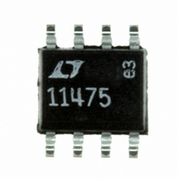
LTC1147CS8-5#PBF Linear Technology, LTC1147CS8-5#PBF Datasheet - Page 12

LTC1147CS8-5#PBF
Manufacturer Part Number
LTC1147CS8-5#PBF
Description
IC SW REG STEP-DOWN 5V 8-SOIC
Manufacturer
Linear Technology
Type
Step-Down (Buck)r
Datasheet
1.LTC1147CN8-3.3.pdf
(16 pages)
Specifications of LTC1147CS8-5#PBF
Internal Switch(s)
No
Synchronous Rectifier
No
Number Of Outputs
1
Voltage - Output
5V
Current - Output
50mA
Frequency - Switching
400kHz
Voltage - Input
3.5 ~ 14 V
Operating Temperature
0°C ~ 70°C
Mounting Type
Surface Mount
Package / Case
8-SOIC (3.9mm Width)
Lead Free Status / RoHS Status
Lead free / RoHS Compliant
Power - Output
-
Available stocks
Company
Part Number
Manufacturer
Quantity
Price
LTC1147-3.3
LTC1147-5/LTC1147L
APPLICATIO S I FOR ATIO
Other losses including C
losses, MOSFET switching losses, and inductor core losses,
generally account for less than 2% total additional loss.
Design Example
As a design example, assume V
3.3V, I
immediately be calculated:
Assume that the MOSFET dissipation is to be limited to
P
If T
50 C/ W, then the junction temperatures will be 63 C and
MOSFET can now be calculated:
The P-channel requirement can be met by a Si9430DY.
Note that the most stringent requirement for the Schottky
diode is with V
continuous short circuit, the worst-case Schottky diode
dissipation rises to:
With the 0.1
increasing the 0.4V Schottky diode dissipation to 0.4W.
C
temperature, and C
optimum efficiency.
Now allow V
voltages the operating frequency will decrease and the
P-channel will be conducting most of the time, causing the
power dissipation to increase. At V
frequency will decrease and the P-channel will be con-
ducting most of the time causing its power dissipation to
increase. At V
12
P
P
IN
R
t
C
L = (5.1)(10
P-Ch R
P
= 0.007(63 – 25) = 0.27. The required R
= 250mW.
A
OFF
will require an RMS current rating of at least 0.5A at
T
SENSE
D
= 50 C and the thermal resistance of the MOSFET is
= 2.61 s/(1.3)(10
= I
MAX
= (1/130kHz)[1 – (3.3/5)] = 2.61 s
SC(AVG)
DS(ON)
= 100mV/1A = 0.1
= 1A, and f = 130kHz; R
IN
IN(MIN)
to drop to its minimum value. At lower input
5
sense resistor I
)(0.1 )(220pF)(3.3V) = 33 H
OUT
(V
=
U
D
OUT
3.3(1)
)
= 4.5V:
= 0 (i.e., short circuit). During a
4
5(0.25)
will require an ESR of 0.1
) = 220pF
U
IN
2
(1.27)
and C
IN
SC(AVG)
= 5V (nominal), V
= 0.3
W
OUT
SENSE
IN(MIN)
= 1A will result,
ESR dissipative
, C
DS(ON)
T
= 4.5V, the
and L can
U
for the
OUT
for
=
This last step is necessary to assure that the power
dissipation and junction temperature of the P-channel are
not exceeded.
Troubleshooting Hints
Since efficiency is critical to LTC1147 series applications,
it is very important to verify that the circuit is functioning
correctly in both continuous and Burst Mode operation.
The waveform to monitor is the voltage on the timing
capacitor Pin 2.
In continuous mode (I
pin should be a sawtooth with a 0.9V
voltage should never dip below 2V as shown in Figure 6a.
When load currents are low (I
operation occurs. The voltage on the C
ground for periods of time as shown in Figure 6b. During
this time the LTC1147 series are in sleep mode with the
quiescent current reduced to 160 A.
The inductor current should also be monitored. Look to
verify that the peak-to-peak ripple current in continuous
mode operation is approximately the same as in Burst
Mode operation.
If Pin 2 is observed falling to ground at high output
currents, it indicates poor decoupling or improper ground-
ing. Refer to the Board Layout Checklist.
f
P
MIN
P
Figure 6a. Continuous Mode Operation C
=
=
Figure 6b. Burst Mode Operation C
3.3(0.125 )(1A)
2.61 s
1
1 –
4.5
LOAD
3.3
4.5
2
> I
(1.27)
= 102kHz
BURST
LOAD
= 116mW
) the voltage on the C
< I
BURST
T
T
Waveform
P-P
pin now falls to
T
Waveform
) Burst Mode
swing. This
sn1147 1147fds
LTC1147 • F06
0V
3.3V
3.3V
0V
T


