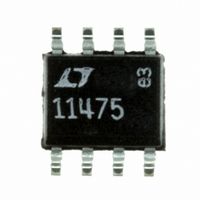
LTC1147CS8-5#PBF Linear Technology, LTC1147CS8-5#PBF Datasheet - Page 6

LTC1147CS8-5#PBF
Manufacturer Part Number
LTC1147CS8-5#PBF
Description
IC SW REG STEP-DOWN 5V 8-SOIC
Manufacturer
Linear Technology
Type
Step-Down (Buck)r
Datasheet
1.LTC1147CN8-3.3.pdf
(16 pages)
Specifications of LTC1147CS8-5#PBF
Internal Switch(s)
No
Synchronous Rectifier
No
Number Of Outputs
1
Voltage - Output
5V
Current - Output
50mA
Frequency - Switching
400kHz
Voltage - Input
3.5 ~ 14 V
Operating Temperature
0°C ~ 70°C
Mounting Type
Surface Mount
Package / Case
8-SOIC (3.9mm Width)
Lead Free Status / RoHS Status
Lead free / RoHS Compliant
Power - Output
-
Available stocks
Company
Part Number
Manufacturer
Quantity
Price
LTC1147-3.3
LTC1147-5/LTC1147L
OPERATIO
APPLICATIO S I FOR ATIO
LTC1147L Adjustable Applications
When an output voltage other than 3.3V or 5V is required,
the LTC1147L adjustable version is used with an external
resistive divider from V
The regulated voltage is determined by:
The LTC1147 series uses a current mode, constant off-
time architecture to switch an external P-channel power
MOSFET. Operating frequency is set by an external capaci-
tor at C
The output voltage is sensed by an internal voltage divider
connected to SENSE
a gain block G, compare the divided output voltage with a
reference voltage of 1.25V. To optimize efficiency, the
LTC1147 series automatically switchs between two modes
of operation, burst and continuous. The voltage compara-
tor is the primary control element when the device is in
Burst Mode operation, while the gain block controls the
output voltage in continuous mode.
During the switch “on” cycle in continuous mode, current
comparator C monitors the voltage between Pins 4 and 5
connected across an external shunt in series with the
inductor. When the voltage across the shunt reaches its
threshold value, the PDRIVE output is switched to V
turning off the P-channel MOSFET. The timing capacitor
connected to Pin 2 is now allowed to discharge at a rate
determined by the off-time controller. The discharge cur-
rent is made proportional to the output voltage (measured
by Pin 4) to model the inductor current, which decays at
a rate which is also proportional to the output voltage.
When the voltage on the timing capacitor has discharged
past V
causes the PDRIVE output to go low turning the P-channel
MOSFET back on. The cycle then repeats.
As the load current increases, the output voltage de-
creases slightly. This causes the output of the gain stage
6
V
OUT
TH1
T
= 1.25
(Pin 2).
, comparator T trips, setting the flip-flop. This
1 +
U
U
–
(Pin 4). A voltage comparator V, and
R2
R1
(Refer to Functional Diagram)
OUT
U
to V
FB
(Pin 6) (see Figure 7).
W
U
IN
,
(Pin 3) to increase the current comparator threshold, thus
tracking the load current.
The sequence of events for Burst Mode operation is very
similar to continuous operation with the cycle interrupted
by the voltage comparator. When the output voltage is at
or above the desired regulated value, the P-channel MOS-
FET is held off by comparator V and the timing capacitor
continues to discharge below V
capacitor discharges past V
trips, causing the internal sleep line to go low.
The circuit now enters sleep mode with the power MOS-
FET turned off. In sleep mode, a majority of the circuitry is
turned off, dropping the quiescent current from 1.6mA to
160 A. The load current is now being supplied from the
output capacitor. When the output voltage has dropped by
the amount of hysteresis in comparator V, the P-channel
MOSFET is again turned on and this process repeats.
To avoid the operation of the current loop interfering with
Burst Mode operation, a built-in offset V
in the gain stage. This prevents the current comparator
threshold from increasing until the output voltage has
dropped below a minimum threshold.
Using constant off-time architecture, the operating fre-
quency is a function of the input voltage. To minimize the
frequency variation as dropout is approached, the off-time
controller increases the discharge current as V
below V
turned on continuously (100% duty cycle), providing low
dropout operation with V
To prevent stray pickup a 100pF capacitor is suggested
across R1 located close to the LTC1147L.
For Figure 1 applications with V
R
inputs operate near ground. When the current comparator
is operated at less than 2V common mode, the off-time
increases approximately 40%, requiring the use of a
smaller timing capacitor C
SENSE
is moved to ground, the current sense comparator
OUT
+ 1.5V. In dropout the P-channel MOSFET is
OUT
T
.
TH2
V
, voltage comparator S
IN
OUT
TH1
.
. When the timing
below 2V, or when
OS
is incorporated
sn1147 1147fds
IN
drops


