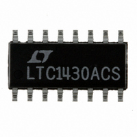
LTC1430ACS Linear Technology, LTC1430ACS Datasheet - Page 16

LTC1430ACS
Manufacturer Part Number
LTC1430ACS
Description
IC SW REG CNTRLR STEP-DWN 16SOIC
Manufacturer
Linear Technology
Type
Step-Down (Buck)r
Datasheet
1.LTC1430ACS8.pdf
(24 pages)
Specifications of LTC1430ACS
Internal Switch(s)
No
Synchronous Rectifier
Yes
Number Of Outputs
1
Voltage - Output
3.3V, Adj
Current - Output
50A
Frequency - Switching
50kHz ~ 500kHz
Voltage - Input
4 ~ 8 V
Operating Temperature
0°C ~ 70°C
Mounting Type
Surface Mount
Package / Case
16-SOIC (3.9mm Width)
Lead Free Status / RoHS Status
Contains lead / RoHS non-compliant
Power - Output
-
Available stocks
Company
Part Number
Manufacturer
Quantity
Price
Company:
Part Number:
LTC1430ACS8
Manufacturer:
LT
Quantity:
10 000
Part Number:
LTC1430ACS8
Manufacturer:
LINEAR/凌特
Quantity:
20 000
Company:
Part Number:
LTC1430ACS8#TRPBF
Manufacturer:
LINEAR
Quantity:
12 711
LTC1430A
internal 20 A source and runs at 200kHz. Connecting a
50k resistor from FREQSET to ground will sink an addi-
tional 25 A from FREQSET, causing the internal oscillator
to run at approximately 450kHz. Sourcing an external
10 A current into FREQSET will cut the internal frequency
to 100kHz. An internal clamp prevents the oscillator from
running slower than about 50kHz. Tying FREQSET to V
will cause it to run at this minimum speed.
Shutdown
The LTC1430A includes a low power shutdown mode,
controlled by the logic at the SHDN pin. A high at SHDN
allows the part to operate normally. A low level at SHDN
stops all internal switching, pulls COMP and SS to ground
internally and turns Q1 and Q2 off. In shutdown, the
LTC1430A itself will drop below 1 A quiescent current
typically, although off-state leakage in the external
MOSFETs may cause the total PV
what higher, especially at elevated temperatures. When
SHDN rises again, the LTC1430A will rerun a soft start
cycle and resume normal operation. Holding the LTC1430A
in shutdown during PV
sequencing constraints.
External Clock Synchronization
The LTC1430A SHDN pin can double as an external clock
input for applications that require a synchronized clock or
a faster switching speed. The SHDN pin terminates the
internal sawtooth wave and resets the oscillator immedi-
ately when it goes low, but waits 50 s before shutting
down the rest of the internal circuitry. A clock signal
applied directly to the SHDN pin will force the LTC1430A
internal oscillator to lock to its frequency as long as the
external clock runs faster than the internal oscillator
frequency. The LTC1430A can be synchronized to fre-
quencies between 250kHz and 350kHz with no additional
components.
The LTC1430A is synchronizable at frequencies from
200kHz to 500kHz. Frequencies above 300kHz can cause
a decrease in the maximum obtainable duty cycle as rise/
fall time and propagation delay take up a large fraction of
the switch cycle. Circuits using these frequencies should
A
16
PPLICATI
O
U
S
CC
I FOR ATIO
power up removes any PV
U
CC
W
current to be some-
U
CC1
CC
be checked carefully in applications where operation near
dropout is important—like 3.3V to 2.5V converters. Fre-
quencies above 500kHz can cause erratic current limit
operation and are not recommended.
LAYOUT CONSIDERATIONS
Grounding
Proper grounding is critical for the LTC1430A to obtain
specified output regulation. Extremely high peak currents
(as high as several amps) can flow between the bypass
capacitors and the PV
currents can generate significant voltage differences be-
tween two points that are nominally both “ground.” As a
general rule, GND and PGND should be totally separated
on the layout, and should be brought together at only one
point, right at the LTC1430A GND and PGND pins. This
helps minimize internal ground disturbances in the
LTC1430A by keeping PGND and GND at the same poten-
tial, while preventing excessive current flow from disrupt-
ing the operation of the circuits connected to GND. The
PGND node should be as compact and low impedance as
possible, with the negative terminals of the input and
output capacitors, the source of Q2, the LTC1430A PGND
node, the output return and the input supply return all
clustered at one point. Figure 14 is a modified schematic
showing the common connections in a proper layout. Note
that at 10A current levels or above, current density in the
PC board itself can become a concern; traces carrying high
currents should be as wide as possible.
Output Voltage Sensing
The 16-lead versions of the LTC1430A provide three pins
for sensing the output voltage: SENSE
SENSE
divider which is connected to FB. To set the output of the
LTC1430A to 3.3V, connect SENSE
to the load as practical and connect SENSE
common GND/PGND point. Note that SENSE
differential input sense input; it is just the bottom of the
internal divider string. Connecting SENSE
near the load will not improve load regulation. For any
other output voltage, the SENSE
+
and SENSE
–
CC1
connect to an internal resistor
, PV
CC2
+
and SENSE
and PGND pins. These
+
to the output as near
+
, SENSE
–
to the ground
–
–
pins should
is not a true
–
–
and FB.
to the


