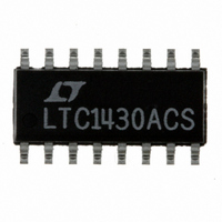
LTC1430ACS Linear Technology, LTC1430ACS Datasheet - Page 8

LTC1430ACS
Manufacturer Part Number
LTC1430ACS
Description
IC SW REG CNTRLR STEP-DWN 16SOIC
Manufacturer
Linear Technology
Type
Step-Down (Buck)r
Datasheet
1.LTC1430ACS8.pdf
(24 pages)
Specifications of LTC1430ACS
Internal Switch(s)
No
Synchronous Rectifier
Yes
Number Of Outputs
1
Voltage - Output
3.3V, Adj
Current - Output
50A
Frequency - Switching
50kHz ~ 500kHz
Voltage - Input
4 ~ 8 V
Operating Temperature
0°C ~ 70°C
Mounting Type
Surface Mount
Package / Case
16-SOIC (3.9mm Width)
Lead Free Status / RoHS Status
Contains lead / RoHS non-compliant
Power - Output
-
Available stocks
Company
Part Number
Manufacturer
Quantity
Price
Company:
Part Number:
LTC1430ACS8
Manufacturer:
LT
Quantity:
10 000
Part Number:
LTC1430ACS8
Manufacturer:
LINEAR/凌特
Quantity:
20 000
Company:
Part Number:
LTC1430ACS8#TRPBF
Manufacturer:
LINEAR
Quantity:
12 711
LTC1430A
APPLICATIONS
OVERVIEW
The LTC1430A is a voltage feedback PWM switching
regulator controller (see Block Diagram) designed for use
in high power, low voltage step-down (buck) converters.
It includes an onboard PWM generator, a precision refer-
ence trimmed to 0.5%, two high power MOSFET gate
drivers and all necessary feedback and control circuitry to
form a complete switching regulator circuit. The PWM
loop nominally runs at 200kHz.
The 16-lead versions of the LTC1430A include a current
limit sensing circuit that uses the upper external power
MOSFET as a current sensing element, eliminating the
need for an external sense resistor.
Also included in the 16-lead version is an internal soft start
feature that requires only a single external capacitor to
operate. In addition, 16-lead parts feature an adjustable
oscillator which can run at frequencies from 50kHz to
500kHz, allowing added flexibility in external component
selection. The 8-lead version does not include current
limit, internal soft start or frequency adjustability.
THEORY OF OPERATION
Primary Feedback Loop
The LTC1430A senses the output voltage of the circuit at
the output capacitor with the SENSE
and feeds this voltage back to the internal transconduc-
tance amplifier FB. FB compares the resistor-divided out-
put voltage to the internal 1.265V reference and outputs an
error signal to the PWM comparator. This is then com-
pared to a fixed frequency sawtooth waveform generated
by the internal oscillator to generate a pulse width modu-
lated signal. This PWM signal is fed back to the external
MOSFETs through G1 and G2, closing the loop. Loop
compensation is achieved with an external compensation
network at COMP, the output node of the FB transconduc-
tance amplifier.
MIN, MAX Feedback Loops
Two additional comparators in the feedback loop provide
high speed fault correction in situations where the FB
amplifier may not respond quickly enough. MIN compares
the feedback signal to a voltage 40mV (3%) below the
8
U
INFORMATION
U
W
+
and SENSE
U
–
pins
internal reference. At this point, the MIN comparator
overrides the FB amplifier and forces the loop to full duty
cycle, set by the internal oscillator at about 93.5%. Simi-
larly, the MAX comparator monitors the output voltage at
3% above the internal reference and forces the output to
0% duty cycle when tripped. These two comparators
prevent extreme output perturbations with fast output
transients, while allowing the main feedback loop to be
optimally compensated for stability.
Current Limit Loop
The 16-lead LTC1430A devices include yet another feed-
back loop to control operation in current limit. The current
limit loop is disabled in the 8-lead device. The I
fier monitors the voltage drop across external MOSFET Q1
with the I
high. It compares this voltage to the voltage at the I
As the peak current rises, the drop across Q1 due to its
R
that Q1’s drain current has exceeded the maximum level,
I
capacitor, cutting the duty cycle and controlling the output
current level. At the same time, the I
generates a signal to disable the MIN comparator to
prevent it from conflicting with the current limit circuit. If
the internal feedback node drops below about 0.8V, indi-
cating a severe output overload, the circuitry will force the
internal oscillator to slow down by a factor of as much as
100. If desired, the turn on time of the current limit loop
can be controlled by adjusting the size of the soft start
capacitor, allowing the LTC1430A to withstand short
overcurrent conditions without limiting.
By using the R
the current limit circuit eliminates the sense resistor that
would otherwise be required and minimizes the number of
components in the external high current path. Because
power MOSFET R
with temperature, the LTC1430A current limit is not de-
signed to be accurate; it is meant to prevent damage to the
power supply circuitry during fault conditions. The actual
current level where the limiting circuit begins to take effect
may vary from unit to unit, depending on the power
MOSFETs used. See Soft Start and Current Limit for more
details on current limit operation.
LIM
DS(ON)
starts to pull current out of the external soft start
increases. When I
FB
pin during the portion of the cycle when G1 is
DS(ON)
DS(ON)
of Q1 to measure the output current,
is not tightly controlled and varies
FB
drops below I
LIM
MAX
comparator
, indicating
LIM
MAX
ampli-
pin.


