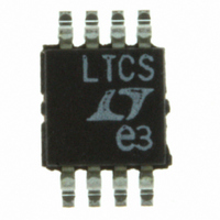
LTC1474CMS8-5#PBF Linear Technology, LTC1474CMS8-5#PBF Datasheet - Page 10

LTC1474CMS8-5#PBF
Manufacturer Part Number
LTC1474CMS8-5#PBF
Description
IC CONV STEP-DWN HI-EFF 8-MSOP
Manufacturer
Linear Technology
Type
Step-Down (Buck)r
Datasheet
1.LTC1474CS8-5PBF.pdf
(20 pages)
Specifications of LTC1474CMS8-5#PBF
Internal Switch(s)
Yes
Synchronous Rectifier
No
Number Of Outputs
1
Voltage - Output
5V
Current - Output
750mA
Voltage - Input
3 ~ 18 V
Operating Temperature
0°C ~ 70°C
Mounting Type
Surface Mount
Package / Case
8-MSOP, Micro8™, 8-uMAX, 8-uSOP,
Lead Free Status / RoHS Status
Lead free / RoHS Compliant
Power - Output
-
Frequency - Switching
-
Available stocks
Company
Part Number
Manufacturer
Quantity
Price
APPLICATIONS
LTC1474/LTC1475
2. I
3. The catch diode loss is due to the V
Adjustable Applications
For adjustable versions, the output voltage is programmed
with an external divider from V
in Figure 4. The regulated voltage is determined by:
10
small that this loss is negligible at loads above a
milliamp but at no load accounts for nearly all of the
loss. The second component, the gate charge current,
results from switching the gate capacitance of the
internal P-channel switch. Each time the gate is switched
from high to low to high again, a packet of charge dQ
moves from V
current out of V
DC bias current. In continuous mode, I
where Q
the DC bias and gate charge losses are proportional to
V
higher supply voltages.
inductor and current sense resistor. At low supply
voltages where the switch on-resistance is higher and
the switch is on for longer periods due to higher duty
cycle, the switch losses will dominate. Keeping the peak
currents low with the appropriate R
larger inductance helps minimize these switch losses.
At higher supply voltages, these losses are proportional
to load and result in the flat efficiency curves seen in
Figure 1.
conducts current during the off-time and is more pro-
nounced at high supply voltage where the on-time is
short. This loss is proportional to the forward drop.
However, as discussed in the Catch Diode section,
diodes with lower forward drops often have higher
leakage current, so although efficiency is improved, the
no load supply current will increase.
V
IN
2
OUT
R losses are predicted from the internal switch,
and thus their effects will be more pronounced at
= 1.23 1+
P
is the gate charge of the internal switch. Both
IN
IN
U
to ground. The resulting dQ/dt is the
which is typically much larger than the
R2
R1
INFORMATION
U
OUT
to V
W
D
FB
I
D
loss as the diode
(Pin 1) as shown
SENSE
GATECHG
U
and with
= fQ
(4)
P
To minimize no-load supply current, resistor values in the
megohm range should be used. The increase in supply
current due to the feedback resistors can be calculated
from:
A 10pF feedforward capacitor across R2 is necessary due
to the high impedances to prevent stray pickup and
improve stability.
Low Battery Comparator
The LTC1474/LTC1475 have an on-chip low battery com-
parator that can be used to sense a low battery condition
when implemented as shown in Figure 5. The resistive
divider R3/R4 sets the comparator trip point as follows:
The divided down voltage at the LBI pin is compared to the
internal 1.23V reference. When V
output sinks current. The low battery comparator is active
all the time, even during shutdown mode.
V
TRIP
I
Figure 4. LTC1474/LTC1475 Adjustable Configuration
VIN
V
IN
1 23 1
R
Figure 5. Low Battery Comparator
V
1
OUT
R4
R3
LBI
R
LTC1474
LTC1475
2
GND
R
R
4
–
+
4
3
LTC1474/LTC1475
V
V
OUT
V
1.23V
REFERENCE
FB
IN
1
LBI
10pF
< 1.23V, the LBO
1474/75 F04
V
OUT
1474/75 F05
LBO
R2
R1


