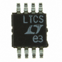
LTC1474CMS8-5#PBF Linear Technology, LTC1474CMS8-5#PBF Datasheet - Page 3

LTC1474CMS8-5#PBF
Manufacturer Part Number
LTC1474CMS8-5#PBF
Description
IC CONV STEP-DWN HI-EFF 8-MSOP
Manufacturer
Linear Technology
Type
Step-Down (Buck)r
Datasheet
1.LTC1474CS8-5PBF.pdf
(20 pages)
Specifications of LTC1474CMS8-5#PBF
Internal Switch(s)
Yes
Synchronous Rectifier
No
Number Of Outputs
1
Voltage - Output
5V
Current - Output
750mA
Voltage - Input
3 ~ 18 V
Operating Temperature
0°C ~ 70°C
Mounting Type
Surface Mount
Package / Case
8-MSOP, Micro8™, 8-uMAX, 8-uSOP,
Lead Free Status / RoHS Status
Lead free / RoHS Compliant
Power - Output
-
Frequency - Switching
-
Available stocks
Company
Part Number
Manufacturer
Quantity
Price
SYMBOL
V
V
I
I
I
R
I
V
V
t
V
V
V
I
I
I
I
I
The
temperature range.
Note 1: T
dissipation P
ELECTRICAL CHARACTERISTICS
FB
SUPPLY
Q
PEAK
OFF
LBO, SINK
RUN, SOURCE
SW, LEAK
LBI, LEAK
LBO, LEAK
FB
OUT
SENSE
HYST
LBI, TRIP
RUN
LBI, OFF
V
ON
OUT
LTC1474CS8/LTC1475CS8: T
LTC1474CMS8/LTC1475CMS8: T
denotes specifications which apply over the full operating
J
is calculated from the ambient temperature T
D
according to the following formulas:
PARAMETER
Feedback Voltage
Regulated Output Voltage
Feedback Current
No Load Supply Current (Note 3)
Output Voltage Line Regulation
Output Voltage Load Regulation
Output Ripple
Input DC Supply Current (Note 2)
Switch Resistance
Current Comp Max Current Trip Threshold
Current Comp Sense Voltage Trip Threshold
Voltage Comparator Hysteresis
Switch Off-Time
Low Battery Comparator Threshold
Run/ON Pin Threshold
OFF Pin Threshold (LTC1475 Only)
Sink Current into Pin 2
Source Current from Pin 8
Switch Leakage Current
Leakage Current into Pin 3
Leakage Current into Pin 2
LTC1474/LTC1475
LTC1474-3.3/LTC1475-3.3
LTC1474-5/LTC1475-5
LTC1474/LTC1475 Only
Active Mode (Switch On)
Sleep Mode (Note 3)
Shutdown
J
= T
J
A
= T
+ (P
A
+ (P
D
• 110 C/W)
D
• 150 C/W)
A
and power
T
A
CONDITIONS
I
I
I
V
I
I
V
V
V
I
R
V
V
V
V
V
V
V
= 25 C, V
(Exclusive of Driver Gate Charge Current)
R
LOAD
LOAD
LOAD
LOAD
LOAD
SW
IN
IN
IN
IN
OUT
OUT
LBI
RUN
IN
LBI
LBI
SENSE
SENSE
= 7V to 12V, I
= 3V to 18V
= 3V to 18V
= 3V to 18V, V
= 18V, V
= 100mA
= 0V, V
= 18V, V
= 2V, V
at Regulated Value
= 0V
= 0V
= 50mA
= 50mA
= 0 (Figure 1 Circuit)
= 0mA to 50mA
= 10mA
= 0
= 1.1
Note 2: Dynamic supply current is higher due to the gate charge being
delivered at the switching frequency. See Applications Information.
Note 3: No load supply current consists of sleep mode DC current (9 A
typical) plus a small switching component (about 1 A for Figure 1 circuit)
necessary to overcome Schottky diode and feedback resistor leakage.
IN
LBO
LBO
SW
IN
= 10V, V
= 18V
= 0V, V
= 0.4V
= 5V
LOAD
RUN
= 0V
= 50mA
RUN
RUN
= 0V
= open, R
SENSE
LTC1474/LTC1475
= 0, unless otherwise noted.
1.205
3.234
4.900
1.16
0.45
MIN
325
3.5
0.4
0.4
0.4
70
90
1.230
3.300
5.000
0.015
4.75
1.23
0.70
TYP
100
400
100
1.4
0.7
0.7
0.8
10
50
76
65
0
5
2
9
6
5
0
0
1.255
3.366
5.100
MAX
1.27
175
110
1.6
6.0
1.0
1.0
1.2
0.1
0.5
30
20
15
15
12
85
1
UNITS
mV
3
mV
mV
mA
mA
mV
mV
mA
P-P
nA
V
V
V
A
A
A
A
V
V
V
A
A
A
A
s
s


