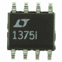
LT1375IS8#PBF Linear Technology, LT1375IS8#PBF Datasheet - Page 6

LT1375IS8#PBF
Manufacturer Part Number
LT1375IS8#PBF
Description
IC SW REG 1.5A ADJ STP-DWN 8SOIC
Manufacturer
Linear Technology
Type
Step-Down (Buck)r
Datasheet
1.LT1376CS8PBF.pdf
(28 pages)
Specifications of LT1375IS8#PBF
Internal Switch(s)
Yes
Synchronous Rectifier
No
Number Of Outputs
1
Voltage - Output
2.42 ~ 21.5 V
Current - Output
1.5A
Frequency - Switching
500kHz
Voltage - Input
5 ~ 25 V
Operating Temperature
-40°C ~ 125°C
Mounting Type
Surface Mount
Package / Case
8-SOIC (3.9mm Width)
Dc To Dc Converter Type
Step Down
Pin Count
8
Input Voltage
25V
Output Voltage
2.42 to 21.5V
Switching Freq
560kHz
Output Current
1.5A
Package Type
SOIC N
Output Type
Adjustable
Switching Regulator
Yes
Line Regulation
0.03%/V
Mounting
Surface Mount
Input Voltage (min)
5V
Operating Temperature Classification
Automotive
Lead Free Status / RoHS Status
Lead free / RoHS Compliant
Power - Output
-
Lead Free Status / Rohs Status
Compliant
Available stocks
Company
Part Number
Manufacturer
Quantity
Price
LT1375/LT1376
TYPICAL PERFORMANCE CHARACTERISTICS
PIN
BOOST: The BOOST pin is used to provide a drive voltage,
higher than the input voltage, to the internal bipolar NPN
power switch. Without this added voltage, the typical
switch voltage loss would be about 1.5V. The additional
boost voltage allows the switch to saturate and voltage
loss approximates that of a 0.3Ω FET structure, but with
much smaller die area. Efficiency improves from 75% for
conventional bipolar designs to > 87% for these new parts.
V
NPN switch. It is driven up to the input pin voltage during
switch on time. Inductor current drives the switch pin
negative during switch off time. Negative voltage is clamped
6
SW
1.50
1.25
1.00
0.75
0.50
0.25
12
10
U
8
6
4
2
0
0
: The switch pin is the emitter of the on-chip power
0
0
Maximum Load Current
at V
BOOST Pin Current
T
V
FUNCTIONS
J
OUT
OUT
= 25°C
0.25
= 10V
5
U
= 10V
SWITCH CURRENT (A)
INPUT VOLTAGE (V)
0.50
10
U
0.75
15
1.00
L = 20µH
L = 10µH
W
20
L = 5µH
1375/76 G16
1375/76 G13
U
1.25
25
1.50
1.25
1.00
0.75
0.50
0.25
1.4
1.2
1.0
0.8
0.6
0.4
–50
0
V
Maximum Load Current
at V
0
C
SHUTDOWN
V
Pin Shutdown Threshold
OUT
–25
OUT
JUNCTION TEMPERATURE (°C)
= 3.3V
5
= 3.3V
0
INPUT VOLTAGE (V)
10
25
with the external catch diode. Maximum negative switch
voltage allowed is – 0.8V.
SHDN: The shutdown pin is used to turn off the regulator
and to reduce input drain current to a few microamperes.
Actually, this pin has two separate thresholds, one at
2.38V to disable switching, and a second at 0.4V to force
complete micropower shutdown. The 2.38V threshold
functions as an accurate undervoltage lockout (UVLO).
This is sometimes used to prevent the regulator from
operating until the input voltage has reached a predeter-
mined level.
50
15
L = 10µH
L = 20µH
L = 5µH
75
20
100
1375/76 G11
1375/76 G14
125
25
1.50
1.25
1.00
0.75
0.50
0.25
0.8
0.6
0.4
0.2
0
0
0
Switch Voltage Drop
0
Maximum Load Current
at V
T
V
J
OUT
= 25°C
0.25
OUT
5
= 5V
= 5V
SWITCH CURRENT (A)
0.50
INPUT VOLTAGE (V)
10
0.75
15
1.00
L = 20µH
L = 10µH
L = 5µH
20
1.25
1375/76 G18
1375/76 G15
13756fd
1.50
25


