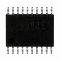
BD9851EFV-E2 Rohm Semiconductor, BD9851EFV-E2 Datasheet

BD9851EFV-E2
Specifications of BD9851EFV-E2
Available stocks
Related parts for BD9851EFV-E2
BD9851EFV-E2 Summary of contents
Page 1
... BD9851EFV Description The BD9850FVM is a 1-channel DC/DC step-down switching regulator controller, while the BD9851EFV is a 2-channel DC/DC step-down switching regulator controller. The BD9850FVM is adaptable for a maximum switching frequency of 2 MHz and the BD9851EFV for that of 3 MHz. Both provide space saving in all applications. ...
Page 2
... Maximum junction temperature Storage temperature * ( )Reduce by 8.0 mW/ ºC over 25ºC (When mounted on PCB of 70mm×70mm×1.6mm) Recommended operating range BD9850FVM Item Power supply voltage Oscillation frequency Operating temperature BD9851EFV Item Power supply voltage Oscillation frequency Timing resistor Timing capacitor Symbol Rating Vcc 10 Tstg – ...
Page 3
BD9850FVM Electrical characteristics (Unless otherwise specified, Ta=25˚C, Vcc=7V, fosc=600kHz) Item [Oscillator block] Oscillation frequency Frequency regulation Oscillator amplitude voltage [Soft start / SW block] CTL/ SS pin sink current CTL / SS pin clamp voltage CTL threshold voltage VCTLTH [PWM ...
Page 4
... BD9851EFV Electrical characteristics (Unless otherwise specified, Ta=25˚C, Vcc=12V, fosc=300kHz, STB=3V) Item [Total device] Standby mode circuit current Operation mode circuit current [Reference voltage block] Output voltage Input stability Load stability Short circuit mode output current [Oscillator block] Oscillation frequency Oscillation frequency regulation ...
Page 5
Characteristic data (BD9850FVM) 1.02 1.015 1.01 1.005 1 0.995 0.99 0.985 0.98 –40 – AMBIENT TEMPERATURE : Ta(˚C) Fig.1 Error Amp threshold voltage vs. Ambient temperature 1000 900 800 700 600 500 400 300 200 100 0 0 ...
Page 6
... AMBIENT TEMPERATURE : Ta(˚C) Fig.7 Error Amp threshold voltage vs. Ambient temperature 1000 Vcc=20V 900 800 700 600 500 400 300 200 100 0 0 0.5 1 1.5 2 2.5 (Vcc-OUT) VOLTAGE : VO(V) Fig.9 (Vcc-OUT) Voltage vs. Output source current 2 ...
Page 7
... Vo2 V REF – 5 INV1 – NON2 + – REF DTC2 OSC CT 3 SCP Tmer 14 Latch Fig.14 BD9851EFV Block diagram Vcc Vcc V RT REF REF TRI Clamper V REF PWM COMP 7 CTL/SS Fig.13 BD9850FVM Block diagram Pin No. Pin name Power supply 1 Vcc 2 OUT ...
Page 8
... When the Vcc voltage falls below 3.8 V (or 3 the BD9851EFV), the output of both channels will be fixed at “OFF” and, at the same time, the DTC pin at “L” level. Hysteresis width of 0.1 V (or 0. the BD9851EFV) is provided for the detection voltage and release voltage of the UVLO in order to prevent malfunctions of the IC which may result from variations in the input voltage due to threshold online ...
Page 9
... Vcc pin voltage waveform 3.8V SCP pin voltage waveform OUT pin voltage waveform Output voltage waveform FB pin voltage Soft start set voltage Oscillator output Fig.15 BD9850FVM Timing chart Output short circuit FB CT DTC 2.3V Fig.16 BD9851EFV Timing chart 9/16 1.5V ...
Page 10
... Setting of output voltage for the step-down application can be calculated by the formula below : Setting procedure Vo = Vthea × ( [V] (Vthea: Error Amp threshold voltage Typ. 1.0 [V]) Setting of output voltage (BD9851EFV) Setting procedure • Step-down (CH1), Step-up (CH1) Vo1 = Vthea × ( [V] (Vthea: Error Amp threshold voltage Typ. 1.0 [V]) • ...
Page 11
... Upper : Pin No treated when the CH1 is not used Lower : Pin No treated when the CH2 is not used Fig. 22 Pin treatment procedure for unused channel on BD9851EFV In order to use one channel, treat the pins of unused channel as shown above. Fig. 19 Setting procedure for BD9851EFV oscillation frequency ...
Page 12
Application circuit / Directions for pattern layout (BD9850FVM) Vo Vcc Vcc C1 * OUT GND C2 1µ REF 1 SEL1 GND 2 RT STB 3 CT VCC 4 NON2 V REF 5 INV2 INV1 6 FB2 FB1 7 ...
Page 13
... REF REF REF REF CT 14PIN (SCP) V Vcc V Vcc REF REF SCP 17PIN (V ) REF Vcc Vcc V REF Fig.27 Equivalent circuit (BD9851EFV) 13/16 7,13PIN (DTC2,DTC1) Vcc Vcc DTC 4PIN (NON2) V Vcc Vcc REF NON2 5,16PIN (INV2,INV1) V REF Vcc Vcc INV 19PIN (STB) Vcc ...
Page 14
IC pin input 8) This monolithic IC contains P+ isolation and P substrate layers between adjacent elements to keep them isolated. Pin junctions are formed at the intersection of these P layers with the N layers of other elements, creating ...
Page 15
Although ROHM is confident that the example application circuit reflects the best possible recommendations, be sure to verify circuit 11) characteristics for your particular application. Modification of constants for other externally connected circuits may cause variations in both static and ...
Page 16
Catalog No.08T679A '08.9 ROHM © ...
Page 17
Appendix No copying or reproduction of this document, in part or in whole, is permitted without the consent of ROHM CO.,LTD. The content specified herein is subject to change for improvement without notice. The content specified herein is for the ...


