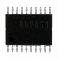
BD9851EFV-E2 Rohm Semiconductor, BD9851EFV-E2 Datasheet - Page 10

BD9851EFV-E2
Manufacturer Part Number
BD9851EFV-E2
Description
IC REG CTRLR SW 2-CH HTSSOP-B20
Manufacturer
Rohm Semiconductor
Type
Step-Down (Buck), Step-Up (Boost), Invertingr
Specifications of BD9851EFV-E2
Internal Switch(s)
No
Synchronous Rectifier
No
Number Of Outputs
2
Current - Output
200mA
Frequency - Switching
10kHz ~ 3MHz
Voltage - Input
4 ~ 18 V
Operating Temperature
-40°C ~ 85°C
Mounting Type
Surface Mount
Package / Case
20-TSSOP Exposed Pad, 20-eTSSOP, 20-HTSSOP
Power - Output
1W
Primary Input Voltage
18V
No. Of Outputs
2
Output Current
200mA
Voltage Regulator Case Style
HTSSOP
No. Of Pins
20
Operating Temperature Range
-40°C To +85°C
Svhc
No SVHC (18-Jun-2010)
Base
RoHS Compliant
Lead Free Status / RoHS Status
Lead free / RoHS Compliant
Voltage - Output
-
Lead Free Status / RoHS Status
Lead free / RoHS Compliant
Other names
BD9851EFV-E2TR
Available stocks
Company
Part Number
Manufacturer
Quantity
Price
Part Number:
BD9851EFV-E2
Manufacturer:
ROHM/罗姆
Quantity:
20 000
Description of external components
Setting of output voltage (BD9851EFV)
Setting of oscillation frequency (BD9850FVM)
Connecting a resistor to the RT pin (pin 2) allows for the setting of oscillation frequency.
• Setting of output voltage (BD9850FVM)
Setting of output voltage for the step-down application can be calculated by the formula below :
10000
1000
100
Vo = Vthea × (R1 + R2) / R2 [V]
(Vthea: Error Amp threshold voltage Typ. 1.0 [V])
• Step-down (CH1), Step-up (CH1)
• Step-down (CH2)
• Inverting (CH2)
Vo1 = Vthea × (R1 + R2) / R2 [V]
Vo2 = 2.5 – {(2.5 - V
V
(Vthea: Error Amp threshold voltage Typ. 1.0 [V])
However, set the INV2 pin voltage to 0.3 to 2.0 V
Vo2 = V
V
However, set the NON2 pin voltage to 0.3 to 2.0 V.
INV
1
NON
2 = 2.5 × R4 / (R3 + R4) [V]
2 = 2.5 × R4 / (R3 + R4) [V]
Fig.18 RT vs. Oscillation frequency
NON
2 × (R1 + R2) / R2 [V]
Timing resistance(RT) [kΩ]
10
INV
Setting procedure
Setting procedure
2) X (R1 + R2) / R1} [V]
100
1000
10/16
Fig.17 Setting procedure for BD9850FVM
oscillation frequency
R
RT
Vo
Vo2
Vo2
RT (2)
Vo1
R1
R2
R1
R2
R1
R2
R1
R2
Application
Application
R4
R3
R3
R4
INV (5)
INV1 (16)
V
NON2 (4)
INV2 (5)
V
INV2 (5)
NON2 (4)
REF
REF
(17)
(17)


