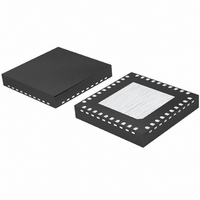
BD95500MUV-E2 Rohm Semiconductor, BD95500MUV-E2 Datasheet - Page 19

BD95500MUV-E2
Manufacturer Part Number
BD95500MUV-E2
Description
IC BUCK ADJ 6A 40VQFN
Manufacturer
Rohm Semiconductor
Type
Step-Down (Buck)r
Datasheet
1.BD95500MUV-E2.pdf
(20 pages)
Specifications of BD95500MUV-E2
Internal Switch(s)
Yes
Synchronous Rectifier
No
Number Of Outputs
1
Voltage - Output
0.7 ~ 5 V
Current - Output
6A
Frequency - Switching
30kHz ~ 100kHz
Voltage - Input
3 ~ 20 V
Operating Temperature
-10°C ~ 100°C
Mounting Type
Surface Mount
Package / Case
40-VQFN
Power - Output
4.66W
Output Voltage
7 V
Output Current
6 A
Input Voltage
3 V to 20 V
Switching Frequency
200 KHz to 1000 KHz
Operating Temperature Range
- 10 C to + 100 C
Mounting Style
SMD/SMT
Lead Free Status / RoHS Status
Lead free / RoHS Compliant
Other names
BD95500MUV-E2TR
(11) Regarding input pin of the IC
(12) Ground Wiring Pattern
●Power Dissipation
Parasitic element
This monolithic IC contains P+ isolation and P substrate layers between adjacent elements in order to keep them isolated.
P-N junctions are formed at the intersection of these P layers with the N layers of other elements, creating a parasitic diode
or transistor. For example, the relation between each potential is as follows:
Parasitic diodes can occur inevitable in the structure of the IC. The operation of parasitic diodes can result in mutual
interference among circuits, operational faults, or physical damage. Accordingly, methods by which parasitic diodes operate,
such as applying a voltage that is lower than the GND (P substrate) voltage to an input pin, should not be used.
When using both small signal and large current GND patterns, it is recommended to isolate the two ground patterns, placing
a single ground point at the ground potential of application so that the pattern wiring resistance and voltage variations
caused by large currents do not cause variations in the small signal ground voltage. Be careful not to change the GND wiring
pattern of any external components, either.
Pin A
5.0
4.5
4.0
3.5
3.0
2.5
2.0
1.5
1.0
0.5
N
0
P
0
+
④4.66W
③3.77W
②1.00W
①0.54W
N
25
○When GND > Pin A and GND > Pin B, the P-N junction operates as a parasitic diode.
○When GND > Pin B, the P-N junction operates as a parasitic transistor.
GND
Ambient Temperature :Ta [℃]
VQFN040-V6060
P
50
P substrate
P
+
N
Resistor
75
Pin A
100
①IC unit time
②1 layer (Substrate surface copper foil area : 0mm
③4 layer (Substrate surface and bottom copper foil area : 20.2mm
④4 layer (all layers copper foil area : 5505mm
θj-a=231.5℃/W
θj-a=125.0℃/W
θj-a=33.2℃/W
θj-a=26.8℃/W
125
Parasitic
element
Example of IC structure
150
2
nd
Parasitic element
and 3
Pin B
N
19/20
rd
P
copper foil area : 5505mm
+
C
B
N
E
GND
P
P substrate
Transistor (NPN)
P
+
N
2
)
GND
2
)
2
)
Other adjacent elements
Pin B
B
2
C
E
GND
Parasitic
element


