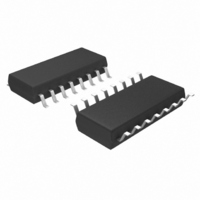
MIC2182-3.3YM Micrel Inc, MIC2182-3.3YM Datasheet - Page 13

MIC2182-3.3YM
Manufacturer Part Number
MIC2182-3.3YM
Description
IC CTRLR SYNC BUCK 3.3V 16-SOIC
Manufacturer
Micrel Inc
Type
Step-Down (Buck)r
Datasheet
1.MIC2182-5.0YSM.pdf
(28 pages)
Specifications of MIC2182-3.3YM
Lead Free Status
Lead free
Internal Switch(s)
No
Synchronous Rectifier
Yes
Number Of Outputs
1
Voltage - Output
3.3V
Current - Output
20A
Frequency - Switching
300kHz
Voltage - Input
4.5 ~ 16.5 V
Operating Temperature
-40°C ~ 85°C
Mounting Type
Surface Mount
Package / Case
16-SOIC (3.9mm Width)
Power - Output
400mW
Number Of Pwm Outputs
1
On/off Pin
Yes
Adjustable Output
No
Topology
Boost/Buck
Switching Freq
330KHz
Operating Supply Voltage (max)
32V
Output Current
20mA
Output Voltage
3.3V
Synchronous Pin
Yes
Rise Time
60ns
Fall Time
60ns
Operating Temperature Classification
Industrial
Mounting
Surface Mount
Pin Count
16
Package Type
SOP N
Duty Cycle
86%
Lead Free Status / RoHS Status
Compliant
Other names
576-1712-5
MIC2182-3.3YM
MIC2182-3.3YM
Available stocks
Company
Part Number
Manufacturer
Quantity
Price
Company:
Part Number:
MIC2182-3.3YM
Manufacturer:
MIC
Quantity:
480
Part Number:
MIC2182-3.3YM
Manufacturer:
MICREL/麦瑞
Quantity:
20 000
Switching from PWM to Skip Mode
The current sense amplifier in Figure 3 monitors the average
voltage across the current-sense resistor. The controller will
switch from PWM to skip mode when the average voltage
across the current-sense resistor drops below approximately
12mV. This is shown in Figure 7b. The average output current
at this transition level for is calculated below.
where:
Switching from Skip to PWM Mode
The frequency of occurrence of the skip-mode current pulses
increase as the output current increases until the hysteretic
duty cycle reaches 100% (continuous pulses). Increasing the
current past this point will cause the output voltage will drop.
The low limit comparator senses the output voltage when it
drops below 2% of the set output and automatically switches
the converter to PWM mode.
The inductor current in skip mode is a triangular wave shape
a minimum value of 0 and a maximum value of 35mV/R
(see Figure 7b). The maximum average output current in skip
mode is the average value of the inductor waveform:
The capacitor on the PWM pin (pin 2) is discharged when the
IC transitions from skip to PWM mode. This forces the IC to
remain in PWM mode for a fixed period of time. The added
delay prevents unwanted switching between PWM and skip
mode. The capacitor is charged with a 10uA current source
on pin 2. The threshold on pin 2 is 2.5V. The delay for a typical
1nF capacitor is:
where:
Current Limit
The current-limit circuit operates during PWM mode. The
output current is detected by the voltage drop across the
external current-sense resistor (R
April 22, 2004
MIC2182
0.012 = threshold voltage of the internal comparator
R
C
I
I
t
OUT(skipmode)
OUT(max skipmode)
delay
CS
PWM
Inductor
= current-sense resistor value
Current
Inductor
= capacitor connected to pin 2
Current
C
PWM
I
source
Figure 7b. Minimum PWM-Mode-Load Inductor Current for PWM Operation
I
0.012
V
MIN(PWM)
R
threshold
I
CS
LIM(skip)
0.5
0A
0A
35mV
Figure 7a. Maximum Skip-Mode-Load Inductor Current
R
CS
CS
1nF 2.5V
10 A
in Figure 2.). The cur-
250 s
CS
13
rent-limit threshold is 100mV+35mV –25mV. The current-
sense resistor must be sized using the minimum current-limit
threshold. The external components must be designed to
withstand the maximum current limit. The current-sense
resistor value is calculated by the equation below:
The maximum output current is:
The current-sense pins CSH (pin 8) and V
noise sensitive due to the low signal level and high input
impedance. The PCB traces should be short and routed close
to each other. A small (1nF to 0.1 F) capacitor across the pins
will attenuate high frequency switching noise.
When the peak inductor current exceeds the current-limit
threshold, the current-limit comparator, in Figure 2, turns off
the high-side MOSFET for the remainder of the cycle. The
output voltage drops as additional load current is pulled from
the converter. When the output voltage reaches approxi-
mately 0.95V, the circuit enters frequency-foldback mode
and the oscillator frequency will drop to 60kHz while maintain-
ing the peak inductor current equal to the nominal 100mV
across the external current-sense resistor. This limits the
maximum output power delivered to the load under a short
circuit condition.
Reference, Enable, and UVLO Circuits
The output drivers are enabled when the following conditions
are satisfied:
The internal bias circuit generates a 1.245V bandgap refer-
ence voltage for the voltage error amplifier and a 5V V
voltage for the gate drive circuit. The reference voltage in the
fixed-output-voltage versions of the MIC2182 is buffered and
brought to pin 7. The V
(pin 4) with a 0.1 F capacitor. The adjustable version of the
MIC2182 uses pin 7 for output voltage sensing. A decoupling
capacitor on pin 7 is not used in the adjustable output voltage
version.
• The V
• The voltage on the enable pin is greater than the
R
I
OUT(max)
undervoltage threshold (typically 4.2V).
enable UVLO threshold (typically 2.5V)
CS
DD
I
OUT(max)
75mV
voltage (pin 11) is greater than its
135mV
R
CS
REF
pin should be bypassed to GND
12mV THRESHOLD
OF AVERAGE VOLTAGE
ACROSS R
35mV THRESHOLD
ACROSS R
CS
.
CS
.
OUT
M9999-042204
(pin 9) are
Micrel
DD


