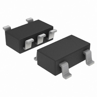
NCP1406SNT1G ON Semiconductor, NCP1406SNT1G Datasheet

NCP1406SNT1G
Specifications of NCP1406SNT1G
NCP1406SNT1GOSTR
Available stocks
Related parts for NCP1406SNT1G
NCP1406SNT1G Summary of contents
Page 1
... ORDERING INFORMATION Device Package Shipping† NCP1406SNT1 TSOP−5 3000 Tape & Reel NCP1406SNT1G TSOP−5 3000 Tape & Reel (Pb−Free) †For information on tape and reel specifications, including part orientation and tape sizes, please refer to our Tape and Reel Packaging Specification Brochure, BRD8011/D ...
Page 2
8.2 mH 2.4 V SUMIDA CR43−8R2MC 1.3 mW VDD FB Enable CE GND R1 110 kW Figure 1. Typical Application Circuit ...
Page 3
Enable Figure 5. Typical 8 V Step−Up Application Circuit FB Bandgap 1.2 V PIN FUNCTION DESCRIPTION Pin Symbol 1 CE Chip Enable Pin (1) The chip is enabled if ...
Page 4
MAXIMUM RATINGS Rating Power Supply Voltage (Pin 3) Input/Output Pin LX (Pin 5) LX Peak Sink Current FB (Pin 2) CE (Pin 1) Input Voltage Range Power Dissipation and Thermal Characteristics Maximum Power Dissipation @ T = 25_C A Thermal ...
Page 5
ELECTRICAL CHARACTERISTICS otherwise noted.) Characteristic ON/OFF TIMING CONTROL Minimum Off Time ( Maximum On Time (Current Not Asserted) Maximum Duty Cycle Minimum Startup Voltage ( mA) OUT Minimum Startup ...
Page 6
V 4 3 OUTPUT CURRENT (mA) OUT Figure 7. Efficiency versus Output Current ( ...
Page 7
T , AMBIENT TEMPERATURE (°C) A Figure 13. Feedback Voltage versus Ambient Temperature 0.18 0.16 0.14 0.12 0.10 0.08 −50 − AMBIENT TEMPERATURE (°C) A Figure 15. ...
Page 8
T , AMBIENT TEMPERATURE (°C) A Figure 19. Soft−start Time versus Ambient Temperature 1.1 1.0 0.9 0.8 0.7 0.6 −50 − AMBIENT TEMPERATURE ...
Page 9
L1 = 8 3.3 mF 5.0 mA OUT OUT V/div 200 mA/div mV/div ...
Page 10
Operation The NCP1406 is a monolithic DC−DC switching converter optimized for single Lithium, two− or three−cell AA/AAA size battery−powered portable products. The NCP1406 operates in a Pulse Frequency Modulation (PFM) scheme with constant peak current control. This scheme maintains high ...
Page 11
The detailed operation of NCP1406 can be best understood by referring to the block diagram and typical application circuits in Figures and 5. The PFM comparator monitors the output voltage via the external feedback resistor divider by ...
Page 12
During shutdown, the IC supply current reduces to 0.3 mA and the LX pin enters high impedance state. However, the input remains connected to the output through the inductor and the Schottky diode, ...
Page 13
The switching frequency at nominal load is expressed as OUT load ) + T ON MAX The maximum output current under this maximum on−time control will be achieved at the limits ...
Page 14
Y5V type ceramic capacitors are not recommended since both their capacitance tolerance and temperature coefficient are too large. The output voltage ripple at nominal load current can be calculated ...
Page 15
Figure 33. Step−Up Converter Demonstration Board Figure 34. Step−Up Converter Demonstration Board Top Layer Copper Top Layer Component Silkscreen Figure 35. Step−Up Converter Demonstration Board http://onsemi.com 15 Bottom Layer Copper ...
Page 16
... Panasonic TDK D1 ON Semiconductor L1 Sumida Electric Co. TDK R1 Panasonic R2 Panasonic U1 ON Semiconductor Part Number Description ECJ2FB0J106M Ceramic Capacitor 0805, 10 mF/6.3 V C1608X5R0J475MT Ceramic Capacitor 0603, 10 mF/6.3 V ECJ3YB1E475M Ceramic Capacitor 1206, 4.7 mF/25 V C3216X5R1E475MT Ceramic Capacitor 1206, 4.7 mF/25 V ECJ1VC1H560K Ceramic Capacitor 0603, 56 pF/50 V ...
Page 17
... Figure 36. Positive−to−Negative Output Converter for Negative LCD Bias 1000 JP1 6 OFF L: CR43−100MC, Sumida C1: ECJ2FB0J106M, Panasonic C2, C5: ECJ3YB1E475M, Panasonic C3: ECJ1VC1H102J, Panasonic C4: ECJ2FB1C225K, Panasonic D1: MBR0520LT1, ON Semiconductor D2, D3: MBR0520LT1 Semiconductor R1: 1.3 MW R2: 110 kW Figure 37. +15 V, −15 V Outputs Converter for LCD Bias Supply C1 2 1000 pF 2.2 mF GND OUT [ * 1.19 ...
Page 18
... V to 5.5 V 820 JP1 6 OFF L: CR43−100MC, Sumida C1: ECJ2FB0J106M, Panasonic C6, C7: ECJ3YB1C106M, Panasonic C3: ECJ1VC1H821J, Panasonic C2, C4, C5: ECJ2FB1C225K, Panasonic D1, D2, D3, D4, D5: MBR0520LT1, ON Semiconductor R1: 1.3 MW R2: 110 kW Figure 38. +15 V, −7.5 V Outputs Converter for CCD Supply Circuit TP1 TP2 6.3 V GND Control Signal ...
Page 19
... C 0.05 H *For additional information on our Pb−Free strategy and soldering details, please download the ON Semiconductor Soldering and Mounting Techniques Reference Manual, SOLDERRM/D. ON Semiconductor and are registered trademarks of Semiconductor Components Industries, LLC (SCILLC). SCILLC reserves the right to make changes without further notice to any products herein. SCILLC makes no warranty, representation or guarantee regarding the suitability of its products for any particular purpose, nor does SCILLC assume any liability arising out of the application or use of any product or circuit, and specifically disclaims any and all liability, including without limitation special, consequential or incidental damages. “ ...


