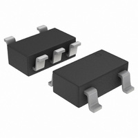
NCP1406SNT1G ON Semiconductor, NCP1406SNT1G Datasheet - Page 12

NCP1406SNT1G
Manufacturer Part Number
NCP1406SNT1G
Description
IC CONV DC-DC 25MA/25V SOT23-5
Manufacturer
ON Semiconductor
Type
Step-Down (Buck), Step-Up (Boost), Invertingr
Datasheet
1.NCP1406SNT1G.pdf
(19 pages)
Specifications of NCP1406SNT1G
Internal Switch(s)
Yes
Synchronous Rectifier
No
Number Of Outputs
1
Voltage - Output
Adj to 25V
Current - Output
25mA
Frequency - Switching
1MHz
Voltage - Input
1.4 ~ 5.5 V
Operating Temperature
-40°C ~ 85°C
Mounting Type
Surface Mount
Package / Case
TSOT-23-5, TSOT-5, TSOP-5
Power - Output
500mW
Mounting Style
SMD/SMT
Lead Free Status / RoHS Status
Lead free / RoHS Compliant
Other names
NCP1406SNT1G
NCP1406SNT1GOSTR
NCP1406SNT1GOSTR
Available stocks
Company
Part Number
Manufacturer
Quantity
Price
Part Number:
NCP1406SNT1G
Manufacturer:
ON/安森美
Quantity:
20 000
the chip is disabled and is shutdown. During shutdown, the
IC supply current reduces to 0.3 mA and the LX pin enters
high impedance state. However, the input remains
connected to the output through the inductor and the
Schottky diode, keeping the output voltage one diode
forward voltage drop below the input voltage.
pin can be pulse width modulated to control LED
brightness.
External Component Selection
Inductor
DCM, the NCP1406 is inherently stable. The inductor
value does not affect the stability of the device. The
NCP1406 is designed to work well with a range of
inductance values; the actual inductance value depends on
the specific application, output current, efficiency, and
output ripple voltage. For step−up conversion, the device
works well with inductance ranging from 1 mH to 47 mH.
The selection of the inductor value along with the load
current, input and output voltages determines the switching
frequency at which the converter will operate.
minimize loss and increase efficiency. It is necessary to
choose an inductor with saturation current greater than the
peak switching current in the application.
frequency, hence increases the losses which yields a lower
overall efficiency.
DCM. Stable operation in CCM is not guaranteed.
the input voltage, T
which is typically 0.9 ms, I
typically 0.8 A, L is the selected inductance, V
desired output voltage, V
voltage, and h is the conversion efficiency which can be
assumed typically 80% for better margin for estimation.
Mode determination
I
following:
expressed as following:
PK
I
L
When the NCP1406 is used to drive white LEDs, the EN
Because it uses a PFM peak current control scheme in
In general, an inductor with small DCR is used to
A lower inductor value increases the switching
As stated before, the NCP1406 is designed to operate in
For all the mathematical equations given below, V
The on−time (inductor ramp up) can be expressed as
The output current and the switching frequency can be
T
ON
T
I
OFF
O
T
T ON +
IDLE
ON_MAX
D
LIM
V IN
L
is the Schottky diode forward
is the current limit which is
is the maximum on−time
I PK
Time
I
D = T
D
PK
2
= T
= V
ON
T
(1 − D)
OFF
IN
SW
OUT
L
T
http://onsemi.com
(eq. 2)
ON
is the
IN
T
SW
is
12
the mode of operation (DCM or CCM). The value of D
will increase as load increases until it reaches 1, which
corresponds to the state of critical conduction when the
inductor current starts ramping up immediately after it
reaches zero (starting a new cycle).
frequency at the critical mode transition (D
expressed as following:
I
If I
the converter operates in continuous conduction mode.
If I
the converter operates in critical conduction mode.
If I
the converter operates in discontinuous conduction mode.
The Discontinuous Conduction Mode
switched on, it will be switched off only when either the
maximum on−time, T
inductor current limit of 0.8 A is met, whichever is earlier.
Therefore, the designer can choose to use either the
maximum on−time or the current limit to turn off the
internal switch.
Minimizing the output ripple voltage
maximum on−time of 0.9 ms should be used to turn off the
MOSFET; however, the maximum output current will be
reduced. It is critical to ensure that the maximum on−time
has been reached before the current limit is met.
be selected according to the following equation:
F SW (load) +
ROOM
In the above equations, D
The value of the output current and the switching
One can determine the mode of operation using the factor
For each switching cycle, if the internal MOSFET is
If the aim is to minimize output ripple voltage, the
To ensure this condition is met, the inductance L should
ROOM
ROOM
ROOM
I OUT +
F SW +
I OUT +
T ON_MAX t L
L u
defined as:
I ROOM +
< 0,
= 0,
> 0,
I LIM
V IN
T ON
V IN
2
2
2
V IN
2
T ON_MAX
T ON
L
L
L
V IN 2
1 ) h
1 * h
ON
V IN
L
V IN 2
, of typical 0.9 ms is reached or the
T ON 2
( V OUT ) V D )
I OUT
2
V OUT )V D
V OUT )V D
( V OUT ) V D )
D 2
I LIM
gives us the information about
1
T ON
V IN
V IN
* 1 )
T ON
D 2
1
1
V OUT ) V D
* 1
V OUT )V D
h
h V IN
h
2
V IN
h * I OUT
= 1) can be
(eq. 3)
(eq. 5)
* 1
(eq. 4)
(eq. 6)
(eq. 7)
2


