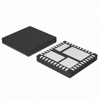
NCP3102BMNTXG ON Semiconductor, NCP3102BMNTXG Datasheet

NCP3102BMNTXG
Specifications of NCP3102BMNTXG
Related parts for NCP3102BMNTXG
NCP3102BMNTXG Summary of contents
Page 1
NCP3102 Wide Input Voltage Synchronous Buck Converter The NCP3102 is a high efficiency DC-DC buck converter designed to operate from 13.2 V supply. The device is capable of producing an output voltage as low ...
Page 2
VCC 13 POR UVLO 0.8V ref COMP DIS RAMP 17 - FAULT + 0.4V 50mV-550mV VOCTH CPHS PIN FUNCTION DESCRIPTION Pin No Symbol 1-4 , 36-40 PWRPHS 5-12 PWRGND 14,15,19,20,23 AGND 16 ...
Page 3
ABSOLUTE MAXIMUM RATINGS Pin Name Control Circuitry Input Voltage Main Supply Voltage Input Bootstrap Supply Voltage Input Phase Node Phase Node (Bootstrap Supply Return) Current Limit Set Feedback COMP/DISABLE MAXIMUM RATINGS Pin Name Thermal Resistance Junction-to-Ambient (Note 2) Operating Junction ...
Page 4
ELECTRICAL CHARACTERISTICS BST = Characteristic Input Voltage Range Boost Voltage Range Quiescent Supply Current V FB Quiescent Supply Current Supply Current Supply Current V CC Boost Quiescent Current V ...
Page 5
TYPICAL OPERATING CHARACTERISTICS 282 281 280 279 278 in 277 276 276 274 - JUNCTION TEMPERATURE (°C) J Figure 4. Oscillator Frequency (F Temperature 801.5 801 ...
Page 6
General NCP3102 is a high efficiency integrated wide input voltage 10 A synchronous PWM buck converter designed to operate from 13.2 V supply. The output voltage of the converter can be precisely regulated down to 800 ...
Page 7
External Soft-Start The NCP3102 features an external soft-start function, which reduces inrush current and overshoot of the output voltage. Soft-Start is achieved by using the internal current source of ...
Page 8
UVLO FAULT + - PWM OUT UVLO FAULT Figure 15. Block Diagram Careful selection and layout of external components is required, to realize the full benefit of the onboard drivers. The capacitors between V ...
Page 9
During a load step transient the output voltage initially drops due to the current variation inside the capacitor and the ESR. (neglecting ...
Page 10
... OTA, the output (eq. 10) capacitor, output inductor and the output divider. Figure 19 shows the open loop and closed loop gain plots possible to use Compensation Calculator Software Tool from ON Semiconductor website. This tool can be downloaded from http://www.onsemi.com. (eq. 11) A 100 Figure 19 ...
Page 11
NCP3102 RLO10 PWRVCC BG PWRPHS Figure 20. Schematic Diagram of NCP3102 Evaluation Board http://onsemi.com 11 NC COMP FB AGND AGND VCC PWRGND PWRGND PWRGND ...
Page 12
Schematic diagram of the NCP3102 demoboard is shown in Figure 20 and the actual PCB layout is shown in Figure 21. The corresponding bill of material is summarized in Table 3. Parameters of the board were tested with Input voltage ...
Page 13
... MULTICOMP 1 MULTICOMP 1 PHYCOMP 1 PHYCOMP 1 1 TYCO ELECT. 1 WELWYN 1 PHYCOMP 1 VISHAY 1 MULTICOMP 1 MULTICOMP 1 MULTICOMP 1 MULTICOMP 1 MULTICOMP 1 MULTICOMP 1 PHYCOMP 1 PHYCOMP 1 PHYCOMP 1 MULTICOMP 2 KEMET 1 SANYO 1 SANYO 2 KEMET 1 AVX 1 AVX 1 TYCHO ELECT. 1 PHYCOMP 1 PHYCOMP 1 AVX 1 AVX 1 ON Semiconducor 2 ON Semiconducor 1 Coilcraft 3 ON Semiconductor 1 ON Semiconductor ...
Page 14
NCP3102 Figure 21. PCB Layout Evaluation Board (110mm x 100mm) http://onsemi.com 14 ...
Page 15
Measured Performance of NCP3102 Demoboard is Shown in Figures 22 Through 25 25° 70° RESISTANCE (kW) ocp ...
Page 16
... Figure 26. Temperature Conditions (V ORDERING INFORMATION Device NCP3102MNTXG NCP3102BMNTXG †For information on tape and reel specifications, including part orientation and tape sizes, please refer to our Tape and Reel Packaging Specifications Brochure, BRD8011/D. NCP3102 = 3 Steady State, No Additional Cooling in out out Package Temperature Grade QFN40 For 0° ...
Page 17
É É É PIN ONE LOCATION É É É É É É É É É TOP VIEW 0.15 C (A3) 0.10 C 0.08 C SIDE VIEW A1 NOTE 40X ...
Page 18
... Opportunity/Affirmative Action Employer. This literature is subject to all applicable copyright laws and is not for resale in any manner. PUBLICATION ORDERING INFORMATION LITERATURE FULFILLMENT: Literature Distribution Center for ON Semiconductor P.O. Box 5163, Denver, Colorado 80217 USA Phone: 303-675-2175 or 800-344-3860 Toll Free USA/Canada Fax: 303-675-2176 or 800-344-3867 Toll Free USA/Canada ...


