NCP3102BMNTXG ON Semiconductor, NCP3102BMNTXG Datasheet - Page 2
NCP3102BMNTXG
Manufacturer Part Number
NCP3102BMNTXG
Description
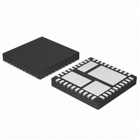
IC CONV SYNC BUCK 10A 40QFN
Manufacturer
ON Semiconductor
Type
Step-Down (Buck)r
Datasheet
1.NCP3102BMNTXG.pdf
(18 pages)
Specifications of NCP3102BMNTXG
Internal Switch(s)
Yes
Synchronous Rectifier
Yes
Number Of Outputs
1
Voltage - Output
Adj to 0.8V
Current - Output
10A
Frequency - Switching
275kHz
Voltage - Input
4.5 ~ 13.2 V
Operating Temperature
-40°C ~ 125°C
Mounting Type
Surface Mount
Package / Case
40-TQFN Exposed Pad
Power - Output
3W
Lead Free Status / RoHS Status
Lead free / RoHS Compliant
Other names
NCP3102BMNTXGOSTR


COMP
PIN FUNCTION DESCRIPTION
DIS
FB
14,15,19,20,23
16
17
1-4 , 36-40
Pin No
26-34
5-12
13
16
17
18
21
22
24
25
35
V
ref
0.8V
-
+
0.4V
-
+
CPHS
UVLO
50mV-550mV
VCC
POR
13
FAULT
VOCTH
COMP/DIS
PWRGND
PWRVCC
PWRPHS
Symbol
TGOUT
AGND
CPHS
TGIN
BST
V
NC
BG
FB
CC
RAMP
CLOCK
OSC
OSC
-
+
-
+
Power phase node. Drain of the low side power MOSFET and source of the high side
MOSFET.
Power ground. Source of the low side power MOSFET. Connected with large copper
area. High current return for the low side MOSFET.
Supply for the internal driver. Decouple with a 0.1 mF - 1 mF capacitor to AGND as close
to the IC as possible.
Internal driver ground. Reference ground for FB, COMP and other driver circuits.
The input pin to the error amplifier.(inverted input error amplifier) Connect this pin to the
output resistor divider (if used) or directly to the output voltage near the load connection.
Compensation or disable pin. (output error amplifier) Use this pin to compensate the
voltage control feedback loop. The compensation capacitor also acts as a soft-start
capacitor. Pulling the pin below 400 mV will disable the controller.
No connect. This pin can be connected to AGND or not connected.
Output high side MOSFET driver.
The controller phase sensing.
Supply rail for the floating top gate driver.
Gate high side MOSFET
Input supply pins for the high side MOSFET. (Drain)
The current limit set pin.
Figure 3. Detailed Block Diagram
R
S
http://onsemi.com
PWM
OUT
NCP3102
2V
LATCH
FAULT
Q
+
2
-
FAULT
FAULT
Description
14,15,19,20,23
BST
24
AGND
VCC
TGOUT
21
+
-
VOCTH
10mA
SET
TGIN
25
2V
35
BG
PWRVCC
PWRGND
26-34
5-12
36-40
1-4
22
PWRPHS
CPHS
Related parts for NCP3102BMNTXG
Image
Part Number
Description
Manufacturer
Datasheet
Request
R

Part Number:
Description:
Wide Input Voltage Synchronous Buck Converter
Manufacturer:
ON Semiconductor
Datasheet:
Part Number:
Description:
ON Semiconductor [VOLTAGE REGULATOR]
Manufacturer:
ON Semiconductor
Datasheet:
Part Number:
Description:
357-036-542-201 CARDEDGE 36POS DL .156 BLK LOPRO
Manufacturer:
ON Semiconductor
Datasheet:
Part Number:
Description:
357-036-542-201 CARDEDGE 36POS DL .156 BLK LOPRO
Manufacturer:
ON Semiconductor
Datasheet:
Part Number:
Description:
357-036-542-201 CARDEDGE 36POS DL .156 BLK LOPRO
Manufacturer:
ON Semiconductor
Datasheet:
Part Number:
Description:
357-036-542-201 CARDEDGE 36POS DL .156 BLK LOPRO
Manufacturer:
ON Semiconductor
Datasheet:
Part Number:
Description:
357-036-542-201 CARDEDGE 36POS DL .156 BLK LOPRO
Manufacturer:
ON Semiconductor
Datasheet:
Part Number:
Description:
357-036-542-201 CARDEDGE 36POS DL .156 BLK LOPRO
Manufacturer:
ON Semiconductor
Datasheet:
Part Number:
Description:
357-036-542-201 CARDEDGE 36POS DL .156 BLK LOPRO
Manufacturer:
ON Semiconductor
Datasheet:
Part Number:
Description:
357-036-542-201 CARDEDGE 36POS DL .156 BLK LOPRO
Manufacturer:
ON Semiconductor
Datasheet:
Part Number:
Description:
357-036-542-201 CARDEDGE 36POS DL .156 BLK LOPRO
Manufacturer:
ON Semiconductor
Datasheet:
Part Number:
Description:
357-036-542-201 CARDEDGE 36POS DL .156 BLK LOPRO
Manufacturer:
ON Semiconductor
Datasheet:
Part Number:
Description:
Manufacturer:
ON Semiconductor
Datasheet:
Part Number:
Description:
Manufacturer:
ON Semiconductor
Datasheet: