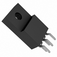
BD9702CP-V5E2 Rohm Semiconductor, BD9702CP-V5E2 Datasheet

BD9702CP-V5E2
Specifications of BD9702CP-V5E2
Related parts for BD9702CP-V5E2
BD9702CP-V5E2 Summary of contents
Page 1
... Single-chip Type with Built-in FET Switching Regulator Series Simple Step-down Switching Regulators with Built-in Power MOSFET BD9701FP/CP-V5/T/T-V5, BD9703FP/CP-V5/T/T-V5,BD9702CP-V5/T/T-V5 ●Description The BD9701/BD9703/BD9702 are single-channel step-down switching regulator capable of PWM operation. The Pch MOS FET is built in for high efficiency in small load area.Lower electricity consumption of operating current 4mA (Typ) and stand-by current 0uA(Typ) is realized by adopting Bi-CMOS process. ● ...
Page 2
... BD9701FP/CP-V5/T/T-V5,BD9703FP/CP-V5/T/T-V5,BD9702CP-V5/T/T-V5 ●Absolute Maximum Ratings (Ta=25℃) Parameter Supply Voltage (VCC-GND) STBY-GND OUT-GND INV-GND Maximum Switching Current Power Dissipation Operating Temperature Storage Temperature *1 Without external heat sink, the power dissipation reduces by 6.4mW/℃ over 25℃. *2 Without external heat sink, the power dissipation reduces by 16.0mW/℃ over 25℃. ...
Page 3
... BD9701FP/CP-V5/T/T-V5,BD9703FP/CP-V5/T/T-V5,BD9702CP-V5/T/T-V5 ●Electrical Characteristics ○BD9703FP/CP-V5/T/T-V5 (Unless otherwise noted, Ta=25℃,VCC=12V,Vo=5V,STBY=3V) Parameter Output ON Resistance Efficiency Switching Frequency Load Regulation Line Regulation Over Current Protection Limit INV Pin Threshold Voltage INV Pin Threshold Voltage Thermal Variation INV Pin Input Current ON STBY Pin Threshold Voltage ...
Page 4
... BD9701FP/CP-V5/T/T-V5,BD9703FP/CP-V5/T/T-V5,BD9702CP-V5/T/T-V5 ●Characteristic Data ○BD9701FP/CP-V5/T/T-V5 100 100 OUTPUT CURRENT : IOUT[A] Fig.1 EFFICIENCY-LOAD CURRENT 5.1 V VCC=30 5. VCC=20 VCC=10 4.9 0 200 400 600 800 OUTPUT CURRENT : IOUT[A] Fig.4 OUTPUT VOLTAGE-LOAD CURRENT 3.5 3 2.5 2 1 0.5 1 1.5 SWITCHING CURRENT : ISW[A] Fig.7 VOUT~OUT VOLTAGE-DRAIN CURRENT www.rohm.com © ...
Page 5
... BD9701FP/CP-V5/T/T-V5,BD9703FP/CP-V5/T/T-V5,BD9702CP-V5/T/T-V5 ●Characteristic Data ○BD9702FP/CP-V5/T/T-V5 100 100 1000 OUTPUT CURRENT : IOUT[A] Fig.10 EFFICIENCY-LOAD CURRENT 5.10 VCC=30V 5.05 VCC=20V 5.00 4.95 VCC=10V 4.90 0 500 1000 1500 2000 2500 3000 OUTPUT CURRENT : IOUT[A] Fig.13 OUTPUT VOLTAGE-LOAD CURRENT 2.0 1.5 1.0 0.5 0.0 0 0 ...
Page 6
... BD9701FP/CP-V5/T/T-V5,BD9703FP/CP-V5/T/T-V5,BD9702CP-V5/T/T-V5 ●Characteristic Data ○BD9703FP/CP-V5/T/T-V5 100 100 OUTPUT CURRENT : IOUT[A] Fig.19 EFFICIENCY-LOAD CURRENT 5.1 VCC=30V 5.05 5 VCC=20V 4.95 VCC=10V 4.9 0 200 400 600 800 1000 OUTPUT CURRENT : IOUT[A] Fig.22 OUTPUT VOLTAGE-LOAD CURRENT 1 0.2 0.4 0.6 0.8 1 1.2 1.4 1.6 SWITCHING CURRENT : ISW[A] Fig.25 VOUT~ ...
Page 7
... BD9701FP/CP-V5/T/T-V5,BD9703FP/CP-V5/T/T-V5,BD9702CP-V5/T/T-V5 ●Block Diagram BD9701FP/CP-V5/T/T-V5, BD9703FP/CP-V5/T-V5, BD9702CP-V5/T/T-V5 TO252-5 Package Dimensions (mm) TO220CP-V5 Package Dimensions (mm) TO220FP-5 Package Dimensions (mm) www.rohm.com © 2009 ROHM Co., Ltd. All rights reserved. VCC 1 VREF PWM COMP OSC STBY 5 STBY TSD Error AMP 3 GND Fig.28 Block Diagram ●Pin Description Pin No. ...
Page 8
... BD9701FP/CP-V5/T/T-V5,BD9703FP/CP-V5/T/T-V5,BD9702CP-V5/T/T-V5 ●Block Function Explanations ・VREF Generates the regulated voltage from VCC input, compensated for temperature. ・OSC Generates the triangular wave oscillation frequency using an internal resistors and capacitor. Used for PWM comparator input. ・Error AMP This block, via the INV pin, detects the resistor-divided output voltage, compares this with the reference voltage, then amplifies and outputs the difference. ・ ...
Page 9
... BD9701FP/CP-V5/T/T-V5,BD9703FP/CP-V5/T/T-V5,BD9702CP-V5/T/T-V5 ●Notes for PCB layout C1 • Place capacitors between VCC and Ground, and the Schottky diode as close as possible to the IC to reduce noise and maximize efficiency. • Connect resistors between INV and Ground, and the output capacitor filter at the same Ground potential in order to stabilize the output voltage. ● ...
Page 10
... BD9701FP/CP-V5/T/T-V5,BD9703FP/CP-V5/T/T-V5,BD9702CP-V5/T/T-V5 ●Recommended Circuit C2 STBY 5 Fig.31 Recommended Circuit Output Voltage 5V : Application cicuit example (BD9701FP/CP-V5/T/T-V5) <Recommended Components (Example)> Inductor L1=100μH Schottky Diode Capacitor <Recommended Components example 2> Inductor L1=100μH Schotky Diode Capacitor www.rohm.com © 2009 ROHM Co., Ltd. All rights reserved. ...
Page 11
... BD9701FP/CP-V5/T/T-V5,BD9703FP/CP-V5/T/T-V5,BD9702CP-V5/T/T-V5 (BD9703FP/CP-V5/T/T-V5) <Recommended Components> Inductor L1=47μH Schotky Diode Capacitor (BD9702CP-V5/T/T-V5) <Recommended Components> Inductor L1=47μH Schotky Diode Capacitor ●Test Circuit + Icc Vcc www.rohm.com © 2009 ROHM Co., Ltd. All rights reserved. :CDRH127/LD (sumida) D1 :RB050LA-40 (ROHM) C1=100μF(50V) :Al electric capacitor UHD1H101MPT (nichicon) C2= ...
Page 12
... BD9701FP/CP-V5/T/T-V5,BD9703FP/CP-V5/T/T-V5,BD9702CP-V5/T/T-V5 ●I/O Equivalent Circuit Pin 1 (VCC), Pin 3 (GND) VCC OUT GND ●Notes for use 1. Absolute Maximum Ratings Use of the IC in excess of absolute maximum ratings such as the applied voltage or operating temperature range may result in IC deterioration or damage. Assumptions should not be made regarding the state of the IC (short mode or open mode) when such damage is suffered ...
Page 13
... BD9701FP/CP-V5/T/T-V5,BD9703FP/CP-V5/T/T-V5,BD9702CP-V5/T/T- pin input This monolithic IC which (as below) has P+ substrate and betweenthe various pin. A P-N junction is formed from this P layer of each pin. For example the relation between each potential is as follows. (When GND > PinB and GND > PinA, the P-N junction operates as a parasitic diode.) Parasitic diodes can occur inevitably in the structure of the IC. The operation of parasitic diodes can result in mutual interference among circuits as well as operation faults and physical damage ...
Page 14
... BD9701FP/CP-V5/T/T-V5,BD9703FP/CP-V5/T/T-V5,BD9702CP-V5/T/T-V5 11. Application circuit Although we can recommend the application circuits contained herein with a relatively high degree of confidence, we ask that you verify all characteristics and specifications of the circuit as well as performance under actual conditions. Please note that we cannot be held responsible for problems that may arise due to patent infringements or noncompliance with any and all applicable laws and regulations ...
Page 15
... BD9701FP/CP-V5/T/T-V5,BD9703FP/CP-V5/T/T-V5,BD9702CP-V5/T/T-V5 ●Ordering part number Part No. Part No. 9701=36V/1.5A 9702=36V/1.5A 9703=36V/3.0A ●Package specifications TO252-5 2.3±0.2 6.5±0.2 0.5±0.1 C0.5 +0.2 5.1 -0.1 FIN 0.5±0.1 0.5 1.27 1.0±0.2 TO220FP-5 +0.3 10.0 −0.1 4.5 +0.3 φ 3.2±0.1 7.0 −0.1 1.2 ...
Page 16
... BD9701FP/CP-V5/T/T-V5,BD9703FP/CP-V5/T/T-V5,BD9702CP-V5/T/T-V5 TO220FP-5(V5) + 0.3 10.0 − 0.1 4.5 + 0.3 φ 3.2±0.1 7.0 − 0.1 1.2 0.8 0.5±0.1 1.778 8. TO220CP-V5 4.5±0.1 φ3.2±0.1 +0.3 +0.2 10.0 -0.1 2.8 -0.1 0.82±0.1 0.92 1.444 1.778 (2.85) 4.12 www.rohm.com © 2009 ROHM Co., Ltd. All rights reserved. ...
Page 17
No copying or reproduction of this document, in part or in whole, is permitted without the consent of ROHM Co.,Ltd. The content specified herein is subject to change for improvement without notice. The content specified herein is for the purpose ...


