BD9702CP-V5E2 Rohm Semiconductor, BD9702CP-V5E2 Datasheet - Page 2
BD9702CP-V5E2
Manufacturer Part Number
BD9702CP-V5E2
Description
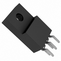
IC REG SW W/MOSFET TO220-5
Manufacturer
Rohm Semiconductor
Type
Step-Down (Buck)r
Specifications of BD9702CP-V5E2
Internal Switch(s)
Yes
Synchronous Rectifier
No
Number Of Outputs
1
Voltage - Output
1 ~ 32 V
Current - Output
3A
Frequency - Switching
110kHz
Voltage - Input
8 ~ 36 V
Operating Temperature
-40°C ~ 85°C
Mounting Type
Through Hole
Package / Case
TO-220-5
Power - Output
2W
No. Of Outputs
1
Output Current
3A
Voltage Regulator Case Style
TO-220
No. Of Pins
5
Operating Temperature Range
-40°C To +85°C
Svhc
No SVHC (18-Jun-2010)
Base Number
9702
Input Voltage Max
35V
Input
RoHS Compliant
Mounting Style
Through Hole
Lead Free Status / RoHS Status
Lead free / RoHS Compliant
Lead Free Status / RoHS Status
Lead free / RoHS Compliant
Other names
BD9702CP-V5E2TR


●Absolute Maximum Ratings (Ta=25℃)
●Operating Conditions(Ta=-40~+85℃)
●Electrical Characteristics
© 2009 ROHM Co., Ltd. All rights reserved.
BD9701FP/CP-V5/T/T-V5,BD9703FP/CP-V5/T/T-V5,BD9702CP-V5/T/T-V5
www.rohm.com
*1 Without external heat sink, the power dissipation reduces by 6.4mW/℃ over 25℃.
*2 Without external heat sink, the power dissipation reduces by 16.0mW/℃ over 25℃.
Reduced by 160mW/℃, when mounted on Infinity size heatsink.
*3The minimum value of an input voltage is the higher either 8.0V or Vo+3
○BD9701FP/CP-V5/T/T-V5 (Unless otherwise noted, Ta=25℃,VCC=12V,Vo=5V,STBY=3V)
This product is not designed to be resistant to radiation.
Input Voltage
Output Voltage
Output ON Resistance
Efficiency
Switching Frequency
Load Regulation
Line Regulation
Over Current Protection Limit
INV Pin Threshold Voltage
INV Pin Threshold Voltage
Thermal Variation
INV Pin Input Current
STBY Pin
Threshold Voltage
STBY Pin Input Current
Circuit Current
Stand-by Current
Maximum Switching Current
Power Dissipation
Parameter
Parameter
Supply Voltage (VCC-GND)
Operating Temperature
Storage Temperature
STBY-GND
Parameter
OUT-GND
INV-GND
OFF
ON
BD9701/BD9703
BD9702
TO252
TO220
VSTBYOFF
ΔVOLOAD
VSTBYON
ΔVOLINE
Symbol
Symbol
ΔVINV
VINV
Istby
V
Ron
fosc
Iocp
IINV
Vo
Icc
Ist
CC
η
0.98
2/16
8.0 or Vo+3
MIN
-0.3
1.6
2.0
80
5
-
-
-
-
-
-
-
-
MIN
1.0
Symbol
Limit
1.00
TYP
±0.5
V
100
VCC
Topr
1.0
Tstg
V
86
10
40
25
Iout
V
Pd
(*3)
1
4
0
STBY
-
-
-
INV
O
MAX
1.02
120
100
1.5
0.3
40
36
50
12
5
-
-
-
-
Limit
TYP
-
-
Unit
kHz
mV
mV
mA
μA
μA
μA
%
%
Ω
A
V
V
V
design guarantee
Io=0.5A design guarantee
VCC=20V,Io=0.5~1.5A
VCC=10~30V,Io=1.0A
Tj=0~85℃ design guarantee
VINV=1.0V
STBY=3V
STBY=0V
-55~+150
-40~+85
Ratings
0.8
1.5
36
36
36
10
2
3
(*2)
(*1)
MAX
Conditions
35.0
Technical Note
32
2009.04- Rev.B
Unit
Unit
W
℃
℃
V
V
V
V
A
V
V
Related parts for BD9702CP-V5E2
Image
Part Number
Description
Manufacturer
Datasheet
Request
R

Part Number:
Description:
Manufacturer:
Rohm Semiconductor
Datasheet:
Part Number:
Description:
Manufacturer:
Rohm Semiconductor
Datasheet:
Part Number:
Description:
Manufacturer:
Rohm Semiconductor
Datasheet:
Part Number:
Description:
Manufacturer:
Rohm Semiconductor
Datasheet:
Part Number:
Description:
Manufacturer:
Rohm Semiconductor
Datasheet:
Part Number:
Description:
Manufacturer:
Rohm Semiconductor
Datasheet:
Part Number:
Description:
Manufacturer:
Rohm Semiconductor
Datasheet:
Part Number:
Description:
Manufacturer:
Rohm Semiconductor
Datasheet:
Part Number:
Description:
Manufacturer:
Rohm Semiconductor
Datasheet:
Part Number:
Description:
Manufacturer:
Rohm Semiconductor
Datasheet:
Part Number:
Description:
Manufacturer:
Rohm Semiconductor
Datasheet:
Part Number:
Description:
Manufacturer:
Rohm Semiconductor
Datasheet:

Part Number:
Description:
DIODE SWITCH 80V 25MA SMD5 TR
Manufacturer:
Rohm Semiconductor
Datasheet: