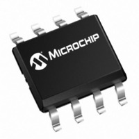
MCP1650S-E/MS Microchip Technology, MCP1650S-E/MS Datasheet - Page 17

MCP1650S-E/MS
Manufacturer Part Number
MCP1650S-E/MS
Description
IC CONTROLLER BOOST 2.55V 8MSOP
Manufacturer
Microchip Technology
Type
Step-Up (Boost), Flyback, Sepicr
Datasheet
1.MCP1650S-EMS.pdf
(28 pages)
Specifications of MCP1650S-E/MS
Internal Switch(s)
No
Synchronous Rectifier
No
Number Of Outputs
1
Frequency - Switching
750kHz
Voltage - Input
2 ~ 5.5 V
Operating Temperature
-40°C ~ 125°C
Mounting Type
Surface Mount
Package / Case
8-MSOP, Micro8™, 8-uMAX, 8-uSOP,
Primary Input Voltage
5.5V
No. Of Outputs
1
Output Voltage
100V
No. Of Pins
8
Operating Temperature Range
-40°C To +125°C
Peak Reflow Compatible (260 C)
Yes
Switching Frequency Max
750kHz
Mounting Style
SMD/SMT
Rohs Compliant
Yes
Lead Free Status / RoHS Status
Lead free / RoHS Compliant
For Use With
MCP1650EV - BOARD EVAL FOR MCP1650,51,52,53MCP1650DM-LED1 - BOARD DEMO FOR MCP165X
Current - Output
-
Voltage - Output
-
Power - Output
-
Lead Free Status / Rohs Status
Lead free / RoHS Compliant
Available stocks
Company
Part Number
Manufacturer
Quantity
Price
Company:
Part Number:
MCP1650S-E/MS
Manufacturer:
MICROCHIP
Quantity:
12 000
5.2
When developing switching power converter circuits,
there are numerous things to consider and the
MCP1650/51/52/53 family is no exception. The gated
oscillator architecture does provide a simple control
approach so that stabilizing the regulator output is an
easier task than that of a fixed-frequency regulator.
The MCP1650/51/52/53 controller utilizes an external
switch and diode allowing for a very wide range of
conversion (high voltage gain and/or high current gain).
There are practical, as well as power-conversion,
topology limitations. The MCP1650/51/52/53 gated
oscillator hysteretic mode converter has similar
limitations, as do fixed-frequency boost converters.
5.2.1
Setting the output voltage:
By adjusting the external resistor divider, the output
voltage of the boost converter can be set to the desired
value. Due to the RC delay caused by the resistor
divider and the device input capacitance, resistor
values greater than 100 k are not recommended. The
feedback voltage is typically 1.22V.
For this example:
90.9 K
Oscillator Frequency = 750 kHz
2004 Microchip Technology Inc.
Where:
Output Voltage = 12V
Output Current = 100 mA
R
R
R
TOP
BOT
V
R
Input Voltage = 2.8V to 4.2V
Design Considerations
was selected as the closest standard value.
OUT
V
BOT
TOP
Duty cycle = 80% for V
Duty cycle = 56% for V
FB
DESIGN EXAMPLE
R
= Top Resistor Value
= Bottom Resistor Value
TO P
= 10 k
= 12V
= 1.22V
= 88.4 k
=
R
BO T
V
-------------
V
OU T
FB
IN
IN
–
< 3.8V
> 3.8V
1
5.2.1.1
For gated oscillator hysteretic designs, the switching
frequency is not constant and will gate several pulses
to raise the output voltage. Once the upper hysteresis
threshold is reached, the gated pulses stop and the
output will coast down at a rate determined by the out-
put capacitor and the load. Using the gated oscillator
switching frequency and duty cycle, it is possible to
determine what the maximum boost ratio is for
continuous inductor current operation.
This relationship assumes that the output load current
is significant and the boost converter is operating in
Continuous Inductor Current mode. If the load is very
light or a small boost inductance is used, higher boost
ratio’s can be achieved.
Calculate at minimum V
The ideal maximum output voltage is 14V. The actual
measured result will be less due to the forward voltage
drop in the boost diode, as well as other circuit losses.
For applications where the input voltage is above and
below 3.8V, another point must be checked to deter-
mine the maximum boost ratio. At 3.8V, the duty cycle
changes from 80% to 56% to minimize the peak current
in the inductor.
For this case, V
12V output specified. The size of the inductor has to
decrease in order to operate the boost regulator in
Discontinuous Inductor Current mode.
Where:
Where:
P
P
P
P
MCP1650/51/52/53
IN
IN
OUT
OUT
= 1.2W/80%
= 1.5 Watts
V
(80% is a good efficiency estimate)
V
= 12V X 100 mA
= 1.2 Watts
OU TMAX
Calculations
OUTMAX
P
IN
OUTMAX
V
P
O UT
OUT
=
P
=
OU T
=
=
=
IN
= 8.63V less than the required
V
:
------------------ -
1 0.56
------------ -
1 D
--------------- -
1 0.8
O UT
–
–
1
–
Efficiency
1
1
I
OU T
V
2.8
IN
3.8
DS21876A-page 17


