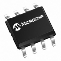
MCP1650S-E/MS Microchip Technology, MCP1650S-E/MS Datasheet - Page 20

MCP1650S-E/MS
Manufacturer Part Number
MCP1650S-E/MS
Description
IC CONTROLLER BOOST 2.55V 8MSOP
Manufacturer
Microchip Technology
Type
Step-Up (Boost), Flyback, Sepicr
Datasheet
1.MCP1650S-EMS.pdf
(28 pages)
Specifications of MCP1650S-E/MS
Internal Switch(s)
No
Synchronous Rectifier
No
Number Of Outputs
1
Frequency - Switching
750kHz
Voltage - Input
2 ~ 5.5 V
Operating Temperature
-40°C ~ 125°C
Mounting Type
Surface Mount
Package / Case
8-MSOP, Micro8™, 8-uMAX, 8-uSOP,
Primary Input Voltage
5.5V
No. Of Outputs
1
Output Voltage
100V
No. Of Pins
8
Operating Temperature Range
-40°C To +125°C
Peak Reflow Compatible (260 C)
Yes
Switching Frequency Max
750kHz
Mounting Style
SMD/SMT
Rohs Compliant
Yes
Lead Free Status / RoHS Status
Lead free / RoHS Compliant
For Use With
MCP1650EV - BOARD EVAL FOR MCP1650,51,52,53MCP1650DM-LED1 - BOARD DEMO FOR MCP165X
Current - Output
-
Voltage - Output
-
Power - Output
-
Lead Free Status / Rohs Status
Lead free / RoHS Compliant
Available stocks
Company
Part Number
Manufacturer
Quantity
Price
Company:
Part Number:
MCP1650S-E/MS
Manufacturer:
MICROCHIP
Quantity:
12 000
MCP1650/51/52/53
6.0
FIGURE 6-1:
When designing the physical layout for the MCP1650/
51/52/53, the highest priority should be placing the
boost power train components in order to minimize the
size of the high current paths. It is also important to pro-
vide ground-path separation between the large-signal
power train ground and the small signal feedback path
and feature grounds. In some cases, additional filtering
on the V
input noise.
In this layout example, the critical power train paths are
from input to output, +V
GND. Current will flow in this path when the switch (Q
is turned on. When Q
flow will quickly change to +V
C
cation, both of these power train paths should be as
short as possible. The C
should all be connected to a single “Power Ground”
plane to minimize any wiring inductance.
Bold traces are used to represent high-current
connections and should be made as wide as is
practical.
R
switching noise on the V
53. This should be considered for high-power
applications (> 1W) and bootstrap applications where
V
voltage of the boost regulator.
DS21876A-page 20
IN
1
1
Single-Cell Li-Ion
Input (2.8V to 4.8V)
to R4 to GND. When starting the layout for this appli-
of the MCP1650/51/52/53 is supplied by the output
and C
TP1
+V
TP4
GND
IN
IN
TYPICAL LAYOUT
_1
pin is helpful to minimize MCP1650/51/52/53
3
FUSE
F1
is an optional filter that reduces the
PGND
0
1
C2
47µ
AGND
MCP1650/51/52/53 Application Schematic.
is turned off, the path for current
2
IN
IN
, Q
R5
73.2K
R8
49.9K
0
_ 1 to F
pin of the MCP1650/51/52/
AGND
1
and R
IN
0
R1
100
C3
0.1µ
_ 1 to F
AGND
(+2.8V to +4.8V Input to +5V Output @ 1A)
2A Power Train Path
1
to C
4
0
GND connections
TP5
/SHDN1
2
1
to L
to L
8
2
6
5
MCP1651_MSOP
Keep Away From Switching Section
V
GND
LBI
/SHDN
1
1
IN
to Q
to D
R2
49.9K
/LBO
EXT
MCP1651R
1
CS
1
FB
to
to
1
DO1813HC
3
1
4
7
)
Coilcraft
3.3 µH
L1
®
The feedback resistor divider that sets the output
voltage should be considered sensitive and be routed
away from the power-switching components discussed
previously.
As shown in the diagram, R
the MCP1650/51/52/53 should be returned to an
analog ground plane.
The analog ground plane and power ground plane
should be connected at a single point close to the input
capacitor (C
PGND
0
Q1
IRLML2502
B330ADIC
D1
AGND
2
).
R3
3.09K
R6
1K
0
VR
562
R7
D2
LED
PGND
0
0.1
Low Input
R4
47µ
C1
TP2
+V
2004 Microchip Technology Inc.
OUT
TP3
GND
6
VR
_1
, R
+5V Output @ 1A
8
and the GND pin of


