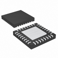
MAX5099ATJ+ Maxim Integrated Products, MAX5099ATJ+ Datasheet - Page 24

MAX5099ATJ+
Manufacturer Part Number
MAX5099ATJ+
Description
IC CONV BUCK SYNC DL 32TQFN-EP
Manufacturer
Maxim Integrated Products
Type
Step-Down (Buck)r
Datasheet
1.MAX5099ATJ.pdf
(27 pages)
Specifications of MAX5099ATJ+
Internal Switch(s)
Both
Synchronous Rectifier
Yes
Number Of Outputs
2
Voltage - Output
0.8 ~ 17.1 V
Current - Output
1A, 2A
Frequency - Switching
200kHz ~ 2.2MHz
Voltage - Input
4.5 ~ 19 V
Operating Temperature
-40°C ~ 125°C
Mounting Type
Surface Mount
Package / Case
32-TQFN Exposed Pad
Power - Output
2.76W
Output Voltage
5.2 V
Output Current
2 A
Input Voltage
5.2 V to 19 V
Supply Current
4.2 mA
Switching Frequency
1.9 MHz
Mounting Style
SMD/SMT
Maximum Operating Temperature
+ 125 C
Minimum Operating Temperature
- 40 C
Lead Free Status / RoHS Status
Lead free / RoHS Compliant
Dual, 2.2MHz, Automotive Synchronous Buck
Converter with 80V Load-Dump Protection
Careful PCB layout is critical to achieve low switching
losses and clean, stable operation. This is especially
true for dual converters where one channel can affect
the other. Refer to the MAX5098A/MAX5099 Evaluation
Kit data sheet for a specific layout example. Use a mul-
tilayer board whenever possible for better noise immu-
nity. Follow these guidelines for good PCB layout:
1) For SGND, use a large copper plane under the IC
2) Isolate the power components and high-current
3) Keep the high-current paths short, especially at the
4) Connect SGND and PGND together at a single
5) Keep the power traces and load connections short.
6) Ensure that the feedback connection to C
7) Route high-speed switching nodes (BST_/VDD_,
24
and solder it to the exposed paddle. To effectively
use this copper area as a heat exchanger between
the PCB and ambient, expose this copper area on
the top and bottom side of the PCB. Do not make a
direct connection from the exposed pad copper
plane to SGND underneath the IC.
path from the sensitive analog circuitry.
ground terminals. This practice is essential for sta-
ble, jitter-free operation.
point. Do not connect them together anywhere else
(refer to the MAX5099 Evaluation Kit data sheet for
more information).
This practice is essential for high efficiency. Use
thick copper PCBs (2oz vs. 1oz) to enhance full-
load efficiency.
short and direct.
SOURCE_) away from the sensitive analog areas
(BYPASS, COMP_, and FB_). Use the internal PCB
layer for SGND as an EMI shield to keep radiated
noise away from the IC, feedback dividers, and
analog bypass capacitors.
______________________________________________________________________________________
PCB Layout Guidelines
OUT
is
1) Place the power components first, with ground ter-
2) Group the gate-drive components (bootstrap
3) Make the DC-DC controller ground connections as
a) Create a signal ground plane underneath the IC.
b) Connect this plane to SGND and use this plane
c) Connect SGND and PGND together (this is the
minals adjacent (inductor, C
all these connections on the top layer with wide,
copper-filled areas (2oz copper recommended).
diodes and capacitors, and V
together near the controller IC.
follows:
for the ground connection for the reference
(BYPASS), enable, compensation components,
feedback dividers, and OSC resistor.
only connection between SGND and PGND).
Refer to the MAX5098A/MAX5099 Evaluation Kit
data sheet for more information.
IN_
Layout Procedure
L
, and C
bypass capacitor)
OUT_
). Make


