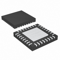
MAX8855ETJ+ Maxim Integrated Products, MAX8855ETJ+ Datasheet

MAX8855ETJ+
Specifications of MAX8855ETJ+
Related parts for MAX8855ETJ+
MAX8855ETJ+ Summary of contents
Page 1
... All-Ceramic-Capacitor Design o 180° Out-of-Phase Operation Reduces Input Ripple Current o Individual Enable Inputs and PWRGD Outputs o Safe-Start into Prebiased Output o Available in 5mm x 5mm Thin QFN Package o Sink/Source Current in DDR Applications PART MAX8855ETJ+ + Denotes a lead(Pb)-free/RoHS-compliant package. Applications * EP = Exposed pad. OUTPUT1 1. OFF Features ...
Page 2
Dual, 5A, 2MHz Step-Down Regulator ABSOLUTE MAXIMUM RATINGS IN_, LX_ VDL, PWRGD_ to GND..................-0.3V to +4. VDL to IN_.....................................................-0.3V to +4.5V DD EN_, SS_, COMP_, FB_, REFIN, FSYNC to GND ......-0.3V to the lower of ...
Page 3
Dual, 5A, 2MHz Step-Down Regulator ELECTRICAL CHARACTERISTICS (continued 3.3V 0.5V, V IN_ VDD VDL FB_ C = 0.022µF, PWRGD_ not connected; T SS_ PARAMETER REFIN, SS2 REFIN Input Bias Current REFIN Common-Mode ...
Page 4
Dual, 5A, 2MHz Step-Down Regulator ELECTRICAL CHARACTERISTICS (continued 3.3V 0.5V, V IN_ VDD VDL FB_ C = 0.022µF, PWRGD_ not connected; T SS_ PARAMETER FSYNC FSYNC Capture Range FSYNC Input Threshold FSYNC ...
Page 5
Dual, 5A, 2MHz Step-Down Regulator ( 3.3V. MAX8855, circuit of Figure 6, T IN1 IN2 SWITCHING FREQUENCY vs. TEMPERATURE 1100 1080 1060 1040 1020 1000 980 960 940 920 900 -40 -15 10 AMBIENT TEMPERATURE (°C) SHUTDOWN ...
Page 6
Dual, 5A, 2MHz Step-Down Regulator ( 3.3V. MAX8855, circuit of Figure 6, T IN1 IN2 OUTPUT PEAK CURRENT LIMIT vs. OUTPUT VOLTAGE 0.8 1.1 1.4 1.7 2.0 2.3 ...
Page 7
Dual, 5A, 2MHz Step-Down Regulator PIN NAME Power-Good Open-Drain Output for Regulator 1. PWRGD1 is high impedance when V ≥ 0 PWRGD1 V FB1 REFIN thermal shutdown is activated, or when V External Reference Input for Regulator ...
Page 8
Dual, 5A, 2MHz Step-Down Regulator PIN NAME Power-Supply Input for Regulator 1. The voltage range is 2.35V to 3.6V. Connect two 10µF and one 0.1µF 27, 28 IN1 ceramic capacitors from IN1 to PGND1. Enable Input for Regulator 1. Drive ...
Page 9
Dual, 5A, 2MHz Step-Down Regulator V DD SHUTDOWN CONTROL BIAS GENERATOR EN1 EN2 VOLTAGE REFERENCE SS1 SOFT-START 1 SS2 SOFT-START 2 + REFIN - FB1 ERROR AMPLIFIER COMP1 COMP LOW DETECTOR FROM SS2 (0.6V FB2 ERROR AMPLIFIER COMP2 ...
Page 10
Dual, 5A, 2MHz Step-Down Regulator The power-good, open-drain output for regulator 2 (PWRGD2) is high impedance when V ≥ 0 PWRGD2 is low when V FB2 SS2 EN2 is low below V ...
Page 11
Dual, 5A, 2MHz Step-Down Regulator For ratiometric tracking applications, connect REFIN to the center of a voltage-divider from the output of regula- tor 2 to GND (see Figure 3b). In this application, the EN_ inputs are connected to each other ...
Page 12
Dual, 5A, 2MHz Step-Down Regulator Figure 3d. Startup and Sequencing Options—Matching Startup Slopes of Output Voltages with Internal Reference In Figure 3d, EN1 and EN2 are connected together and driven as a single input. Although both outputs begin ramping up ...
Page 13
Dual, 5A, 2MHz Step-Down Regulator In DDR tracking applications such as Figure 7, the FB1 regulation voltage tracks the voltage at REFIN. In Figure 7, the output of regulator 1 tracks V of the output voltages is set as follows: ...
Page 14
Dual, 5A, 2MHz Step-Down Regulator Output-Capacitor Selection The key selection parameters for the output capacitor are capacitance, ESR, ESL, and voltage-rating require- ments. These affect the overall stability, output ripple voltage, and transient response of the DC-DC convert- er. The ...
Page 15
Dual, 5A, 2MHz Step-Down Regulator π × × π × × π × ...
Page 16
Dual, 5A, 2MHz Step-Down Regulator Set the second compensation pole at 1/2 the switching frequency. Calculate C10 as follows π × × The recommended range for R4 is 2kΩ to 10kΩ. Note ...
Page 17
Dual, 5A, 2MHz Step-Down Regulator INPUT 2.35V TO 3. 10µF 0.1µF C4 C18 L1 0.1µF 47µF OUT1 0.56µH 0.1µF 1.2V/ 200Ω 10kΩ C11 330pF 10kΩ 1000pF R6 10kΩ C10 OPEN 0.022µF ...
Page 18
Dual, 5A, 2MHz Step-Down Regulator INPUT 2. 10µF 0.1µF C4 C18 L1 0.1µF 47µF OUT1 1µH 0.1µF 0.9V/ 200Ω C9 10kΩ R7 C11 330pF 10kΩ 1000pF OUT2 C10 R1 OPEN 1kΩ R19 ...
Page 19
Dual, 5A, 2MHz Step-Down Regulator Pin Configuration TOP VIEW PGND1 25 PGND1 26 27 IN1 28 IN1 MAX8855 EN1 29 COMP1 30 31 FB1 + 32 SS1 THIN ...
Page 20
... Maxim cannot assume responsibility for use of any circuitry other than circuitry entirely embodied in a Maxim product. No circuit patent licenses are implied. Maxim reserves the right to change the circuitry and specifications without notice at any time. 20 ____________________Maxim Integrated Products, 120 San Gabriel Drive, Sunnyvale, CA 94086 408-737-7600 © 2009 Maxim Integrated Products DESCRIPTION Maxim is a registered trademark of Maxim Integrated Products, Inc ...


