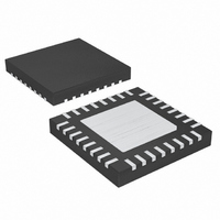
MAX8855ETJ+ Maxim Integrated Products, MAX8855ETJ+ Datasheet - Page 8

MAX8855ETJ+
Manufacturer Part Number
MAX8855ETJ+
Description
IC REG STP DWN DUAL 5A 32-TQFN
Manufacturer
Maxim Integrated Products
Type
Step-Down (Buck)r
Datasheet
1.MAX8855ETJ.pdf
(20 pages)
Specifications of MAX8855ETJ+
Internal Switch(s)
Yes
Synchronous Rectifier
No
Number Of Outputs
2
Voltage - Output
0.6 ~ 3.24 V
Current - Output
5A
Frequency - Switching
500kHz ~ 2MHz
Voltage - Input
2.35 ~ 3.6 V
Operating Temperature
-40°C ~ 85°C
Mounting Type
Surface Mount
Package / Case
32-TQFN Exposed Pad
Power - Output
2.76W
Output Current
5 A
Input Voltage
2.35 V to 3.6 V
Supply Current
2.8 mA
Switching Frequency
2 MHz
Mounting Style
SMD/SMT
Maximum Operating Temperature
+ 85 C
Minimum Operating Temperature
- 40 C
Lead Free Status / RoHS Status
Lead free / RoHS Compliant
Dual, 5A, 2MHz Step-Down Regulator
The controller logic block is the central processor that
determines the duty cycle of the high-side MOSFET
under different line, load, and temperature conditions.
Under normal operation, where the current-limit and
temperature protection are not triggered, the control
logic block takes the output from the PWM comparator
and generates the driver signals for both high-side and
low-side MOSFETs. It also contains the break-before-
make logic and the timing for charging the bootstrap
capacitors. The error signal from the voltage-error
amplifier is compared with the ramp signal generated
by the oscillator at the PWM comparator and, thus, the
required PWM signal is produced. The high-side switch
is turned on at the beginning of the oscillator cycle and
turns off when the ramp voltage exceeds the V
signal or the current-limit threshold is exceeded. The
low-side switch is then turned on for the remainder of
the oscillator cycle. The two switching regulators oper-
ate at the same switching frequency with 180° phase
shift to reduce the input-capacitor ripple current
requirement. Figure 1 shows the MAX8855 functional
diagram.
The MAX8855 provides both peak and valley current limits
to achieve robust short-circuit protection. During the
high-side MOSFET’s on-time, if the drain-source current
reaches the peak current-limit threshold (specified in
the Electrical Characteristics table), the high-side MOS-
FET turns off and the low-side MOSFET turns on, allow-
ing the current to ramp down. At the next clock, the
high-side MOSFET is turned on only if the inductor cur-
8
8
27, 28
_______________________________________________________________________________________
_______________________________________________________________________________________
PIN
29
30
31
32
—
COMP1
NAME
EN1
FB1
SS1
IN1
EP
Power-Supply Input for Regulator 1. The voltage range is 2.35V to 3.6V. Connect two 10µF and one 0.1µF
ceramic capacitors from IN1 to PGND1.
Enable Input for Regulator 1. Drive EN1 high to enable regulator 1, or low for shutdown. For always-on
operation, connect EN1 to V
Compensation for Regulator 1. COMP1 is the output of the internal voltage-error amplifier. Connect external
compensation network from COMP1 to FB1. See the Compensation Design section. COMP1 is internally
pulled to GND when the output is shut down.
Feedback Input for Regulator 1. Connect FB1 to the center of an external resistor-divider from the output to
GND to set the output voltage from 0.6V to 90% of V
Soft-Start for Regulator 1. Connect a capacitor from SS1 to GND to set the startup time. See the Setting the
Soft-Start Time section. When E1 is disabled (pulled low), or regulator 1 is in shutdown mode due to a fault
condition, SS1 is internally pulled low with 335Ω resistor.
Exposed Pad. Connect the exposed pad to the power ground plane.
Detailed Description
PWM Controller
Current Limit
DD
.
COMP_
rent is below the valley current limit. Otherwise, the PWM
cycle is skipped to continue ramping down the inductor
current. When the inductor current stays above the valley
current limit for 12µs and the FB_ is below 0.7 x V
the regulator enters hiccup mode. During hiccup mode,
the SS_ capacitor is discharged to zero and the soft-start
sequence begins after a predetermined time period.
When the V
undervoltage threshold (typically 1.9V), the MAX8855
enters its undervoltage lockout mode (UVLO). UVLO
forces the device to a dormant state until the input volt-
age is high enough to allow the device to function reli-
ably. In UVLO, LX_ nodes of both regulators are in the
high-impedance state. PWRGD1 and PWRGD2 are
forced low in UVLO. When V
undervoltage threshold (typically 2V), the IC powers up
normally as described in the Startup and Sequencing
section.
The UVLO circuitry also monitors the IN1 and IN2 sup-
plies. When the IN_ voltage drops below the falling
undervoltage threshold (typically 1.9V), the correspond-
ing regulator shuts down, and corresponding PWRGD_
goes low. The regulator powers up when V
above the rising undervoltage threshold (typically 2V).
PWRGD1 and PWRGD2 are open-drain outputs that
indicate when the corresponding output is in regulation.
PWRGD1 is high impedance when V
V
0.54V, EN1 is low, V
thermal-overload protection is activated, or when V
< 0.9 x V
FB1
FUNCTION
IN1
≥ 0.9 x V
. FB1 is high impedance when the IC is shut down.
REFIN
Pin Description (continued)
DD
.
REFIN
supply voltage drops below the falling
Undervoltage Lockout (UVLO)
Power-Good Output (PWRGD_)
. PWRGD1 is low when V
VDD
or V
VDD
IN1
rises above the rising
is below V
REFIN
≥ 0.54V and
UVLO
IN_
REFIN
REFIN
rises
, the
FB1
<
,


