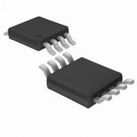
LTC1261LCMS8#TR Linear Technology, LTC1261LCMS8#TR Datasheet - Page 5

LTC1261LCMS8#TR
Manufacturer Part Number
LTC1261LCMS8#TR
Description
IC VOLT INVERT SW CAP ADJ 8MSOP
Manufacturer
Linear Technology
Type
Switched Capacitor (Charge Pump), Invertingr
Datasheet
1.LTC1261LCMS8PBF.pdf
(12 pages)
Specifications of LTC1261LCMS8#TR
Internal Switch(s)
Yes
Synchronous Rectifier
No
Number Of Outputs
1
Voltage - Output
-1.23 ~ -5 V
Current - Output
20mA
Frequency - Switching
650kHz
Voltage - Input
2.7 ~ 5.25 V
Operating Temperature
0°C ~ 70°C
Mounting Type
Surface Mount
Package / Case
8-MSOP, Micro8™, 8-uMAX, 8-uSOP,
Lead Free Status / RoHS Status
Contains lead / RoHS non-compliant
Power - Output
-
Available stocks
Company
Part Number
Manufacturer
Quantity
Price
V
between 2.7V and 5.25V. V
ground with at least a 1 F capacitor placed in close
proximity to the chip. See the Applications Information
section for details.
C1
between C1
C1
from C1
GND (Pin 4): Ground. Connect to a low impedance
ground. A ground plane will help to minimize regulation
errors.
ADJ (COMP for fixed versions) (Pin 5): Output Adjust/
Compensation Pin. For adjustable parts this pin is used
to set the output voltage. The output voltage is divided
down with an external resistor divider and fed back to this
pin to set the regulated output voltage. Typically the
resistor string should draw 10 A from the output to
minimize errors due to the bias current at the adjust pin.
Fixed output voltage parts have the internal resistor
string connected to this pin inside the package. The pin
can be used to trim the output voltage if desired. It can
PIN
5V
TEST CIRCUITS
CC
+
+
–
U
(Pin 1): Power Supply. This requires an input voltage
(Pin 2): C1 Positive Input. Connect a 0.1 F capacitor
(Pin 3): C1 Negative Input. Connect a 0.1 F capacitor
10 F
0.1 F
FUNCTIONS
+
to C1
U
+
and C1
1
2
3
4
–
.
V
C1
C1
GND
CC
LTC1261L-X
+
–
–
U
.
COMP
SHDN
Fixed Output
REG
OUT
8
7
6
5
CC
+
must be bypassed to
1261L TCO1
3.3 F
V
V
OUT
OUT
= – 4V (LTC1261L-4)
= – 4.5V (LTC1261L-4.5)
also be used as an optional feedback compensation pin to
reduce output ripple on both the adjustable and fixed
output voltage parts. See the Applications Information
section for more information on compensation and out-
put ripple.
OUT (Pin 6): Negative Voltage Output. This pin must be
bypassed to ground with a 1 F or larger capacitor. The
value of the output capacitor and its ESR have a strong
effect on output ripple. See the Applications Information
section for more details.
REG (Pin 7): This is an open-drain output that pulls low
when the output voltage is within 5% of the set value. It
will sink 5mA to ground with a 5V supply. The external
circuitry must provide a pull-up or REG will not swing
high. The voltage at REG may exceed V
pulled up to 6V above ground without damage.
SHDN (Pin 8): Shutdown. When this pin is at ground the
LTC1261L operates normally. An internal 5 A pull-down
keeps SHDN low if it is left floating. When SHDN is pulled
high, the LTC1261L enters shutdown mode. In shut-
down, the charge pump is disabled, the output collapses
to 0V and the quiescent current drops to 5 A typically.
0.1 F
V
CC
1
2
3
4
V
C1
C1
GND
CC
Adjustable Output
LTC1261L
+
–
SHDN
REG
OUT
ADJ
8
7
6
5
+
LTC1261L
1261L TCO2
3.3 F
CC
V
and can be
OUT
5


